Symbol Technologies CMOS CXP854P60 User Manual
Page 17
– 17 –
CXP854P60
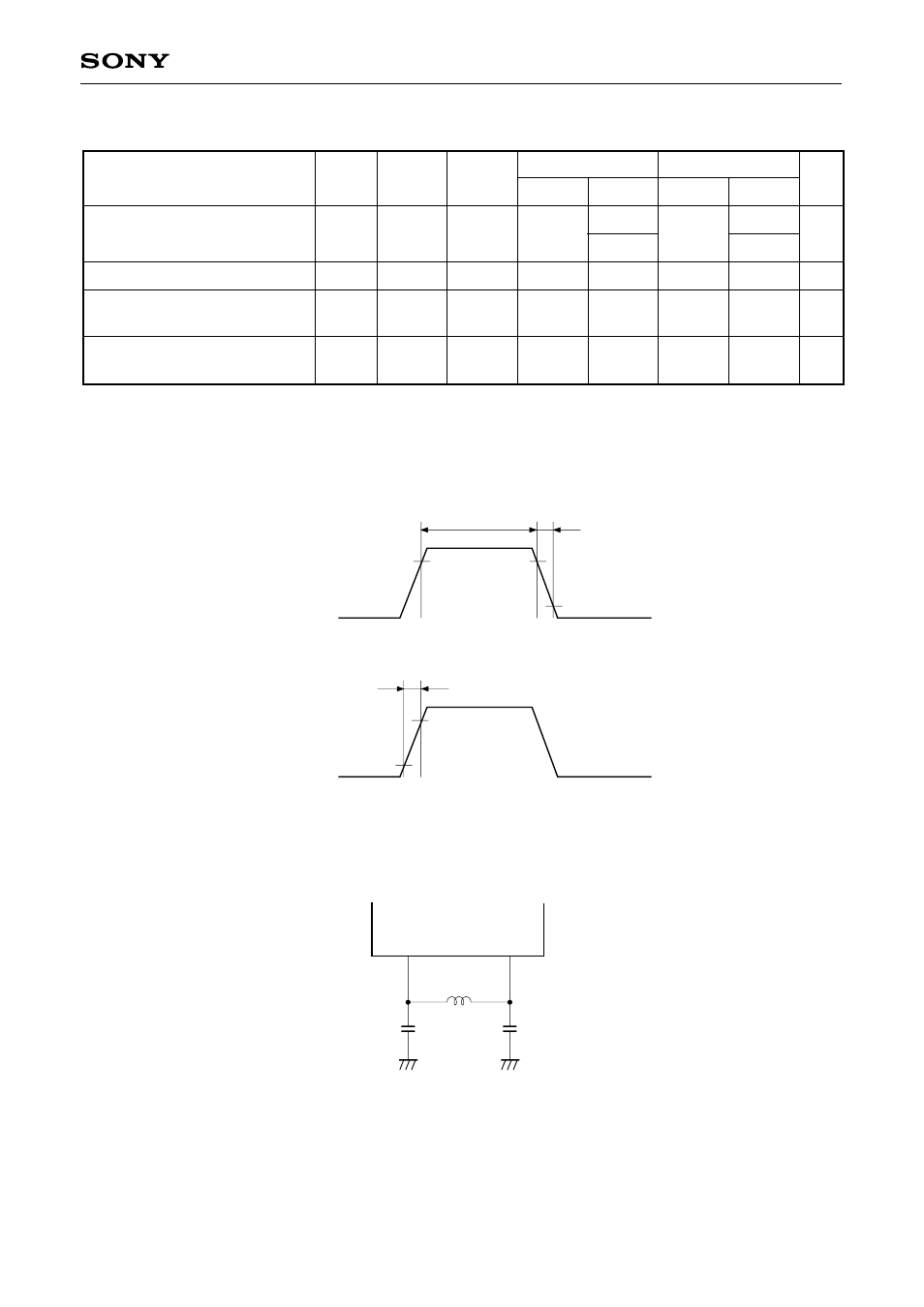
(7) OSD (On Screen Display) timing
(Ta = –10 to +75°C, V
DD
= 4.5 to 5.5V, Vss = 0V)
Item
OSD clock frequency
HSYNC pulse width
HSYNC afterwrite
rise and fall times
VSYNC afterwrite
rise and fall times
f
OSC
t
HWD
t
HCG
t
VCG
EXLC
XLC
HSYNC
HSYNC
VSYNC
Fig. 12
Fig. 11
Fig. 11
Fig. 11
4
1.2
7
∗
1
14
∗
2
200
1.0
4
1.2
MHz
µs
ns
µs
11
∗
1
16
∗
2
200
1.0
Symbol
Pin
Condiiton
Unit
Shadow Existent
Min.
Max.
Min.
Max.
Shadow Non-existent
∗
1
Oscillator clock at 4MHz operation
∗
2
Oscillator clock at 8MHz operation
Fig. 11. OSD timing
0.8V
DD
0.2V
DD
t
HCG
t
HWD
HSYNC
For OPOL register (01FA
H
)
bit 7 at “0”
0.8V
DD
0.2V
DD
t
VCG
VSYNC
For OPOL register (01FA
H
)
bit 6 at “0”
Fig. 12. LC oscillator circuit connection
L
C
2
C
1
EXLC
XLC