Absolute maximum ratings, D c characteristics – Intel 8086-1 User Manual
Page 14
8086
ABSOLUTE MAXIMUM RATINGS
Ambient Temperature Under Bias
0 C to 70 C
Storage Temperature
b
65 C to
a
150 C
Voltage on Any Pin with
Respect to Ground
b
1 0V to
a
7V
Power Dissipation
2 5W
NOTICE This is a production data sheet The specifi-
cations are subject to change without notice
WARNING Stressing the device beyond the ‘‘Absolute
Maximum Ratings’’ may cause permanent damage
These are stress ratings only Operation beyond the
‘‘Operating Conditions’’ is not recommended and ex-
tended exposure beyond the ‘‘Operating Conditions’’
may affect device reliability
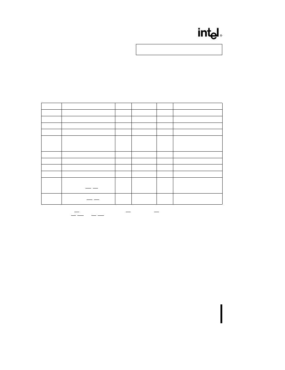
D C CHARACTERISTICS
(8086
T
A
e
0 C to 70 C V
CC
e
5V
g
10%)
(8086-1 T
A
e
0 C to 70 C V
CC
e
5V
g
5%)
(8086-2 T
A
e
0 C to 70 C V
CC
e
5V
g
5%)
Symbol
Parameter
Min
Max
Units
Test Conditions
V
IL
Input Low Voltage
b
0 5
a
0 8
V
(Note 1)
V
IH
Input High Voltage
2 0
V
CC
a
0 5
V
(Notes 1 2)
V
OL
Output Low Voltage
0 45
V
I
OL
e
2 5 mA
V
OH
Output High Voltage
2 4
V
I
OH
e b
400 mA
I
CC
Power Supply Current 8086
340
8086-1
360
mA
T
A
e
25 C
8086-2
350
I
LI
Input Leakage Current
g
10
m
A
0V
s
V
IN
s
V
CC
(Note 3)
I
LO
Output Leakage Current
g
10
m
A
0 45V
s
V
OUT
s
V
CC
V
CL
Clock Input Low Voltage
b
0 5
a
0 6
V
V
CH
Clock Input High Voltage
3 9
V
CC
a
1 0
V
C
IN
Capacitance of Input Buffer
15
pF
fc
e
1 MHz
(All input except
AD
0
– AD
15
RQ GT)
C
IO
Capacitance of I O Buffer
15
pF
fc
e
1 MHz
(AD
0
– AD
15
RQ GT)
NOTES
1 V
IL
tested with MN MX Pin e 0V V
IH
tested with MN MX Pin e 5V MN MX Pin is a Strap Pin
2 Not applicable to RQ GT0 and RQ GT1 (Pins 30 and 31)
3 HOLD and HLDA I
LI
min e 30 mA max e 500 mA
14