6 memory, Memory -19, Memory map -19 – Motorola M68EZ328ADS User Manual
Page 20: Flash memory -19, Interface of flash memories -19, M68vz328ads v2.0 default memory map -19, Freescale semiconductor, i, Freescale semiconductor, inc
Hardware Description and Board Operation
3-19
M68EZ328ADS v2.0 USER’S MANUAL
MOTOROLA
3.6 MEMORY
M68EZ328ADS v2.0 provides on-board Flash memory and EDO DRAM, for application
development. They can be enabled or disabled individually by setting the corresponding DIP
switches.
3.6.1 Memory Map
The default memory map of M68EZ328ADS v2.0 in normal mode is shown in Table 3-5. The
chip select range to all of the memory are software programmable. Users can reconfigure
the memory map for their applications.
3.6.2 FLASH Memory
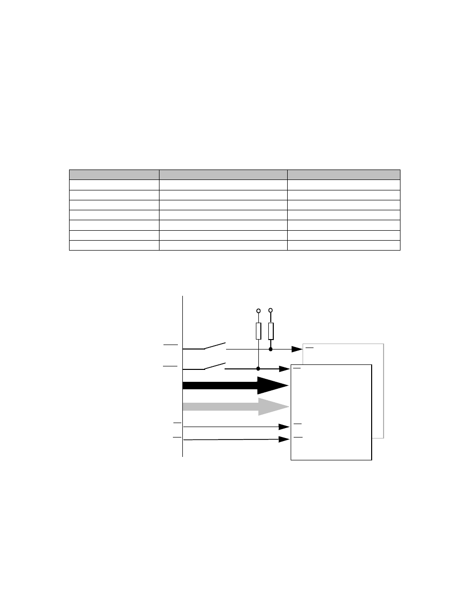
M68EZ328ADS v2.0 supports up to two 2M-byte Flash memory chips. However, only one
bank is installed when the board is shipped out from the factory. Figure 3-2. shows the inter-
face of them. They are chip-selected by *CSA0 and *CSA1 signals. The connection of these
*CSAx signals to the Flash memories is controlled by DIP switches S2-1 and S2-2.
Table 3-5. M68VZ328ADS v2.0 Default Memory Map
System Address
Memory
Assigned Chip Select
$00000000-$007FFFFF
8MB EDO DRAM
CSD0
$00800000-$009FFFFF
2MB FLASH BANK0
CSA0
$00A00000-$00BFFFFF
2MB FLASH BANK1
CSA1
$00C00000-$00FBFFFF
Unused
-
$FFFC0000-$FFFCFFFF
EMU Monitor
EMUCS
$FFFD0000-$FFFDFFFF
Debug Port
EMUCS
$FFFFF000-$FFFFFFFF
MC68EZ328 Internal Register
-
CSA0
OE
WE
1MX16-Bit FLASH
A[0..19]
D[0..15]
CE
OE
WE
1MX16-Bit FLASH
D[0..15]
A[1..20]
CSA1
MC68EZ328
CE
S2-1
S2-2
VCC VCC
FLASH0
FLASH1
Figure 3-2. Interface of Flash Memories
Freescale Semiconductor, I
Freescale Semiconductor, Inc.
For More Information On This Product,
Go to: www.freescale.com
nc.
..
ARCHIVED BY FREESCALE SEMICONDUCTOR, INC. 2005
ARCHIVED BY FREESCALE SEMICONDUCT
OR,
INC.
2005