Table 5. voltage reference modes – Maxim Integrated MAX5865 User Manual
Page 9
Evaluates: MAX5863/MAX5864/MAX5865
MAX5865 Evaluation Kit
_______________________________________________________________________________________
9
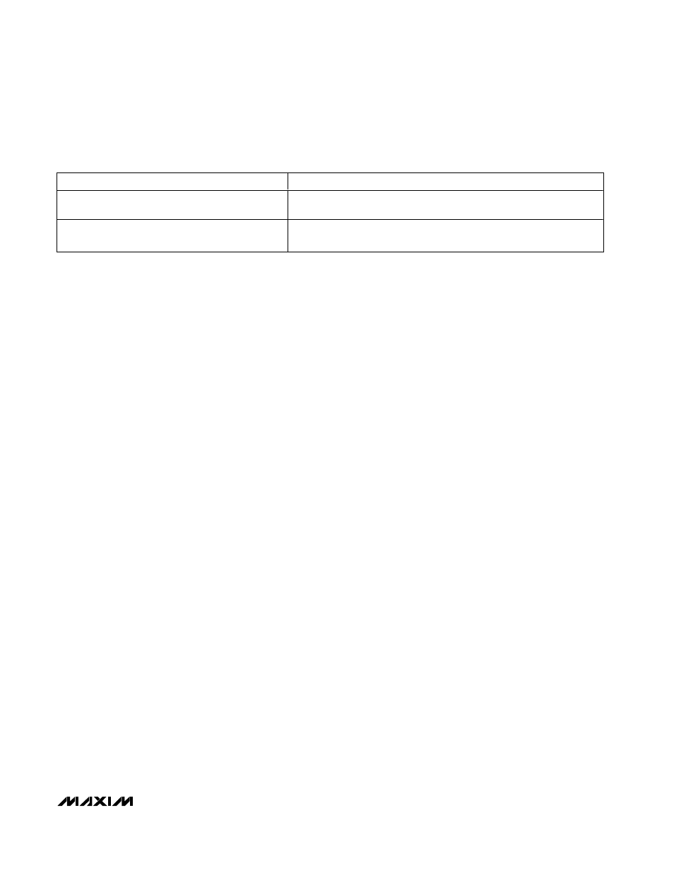
Table 5. Voltage Reference Modes
REFIN VOLTAGE
REFERENCE MODE
VDD
(shunt across jumper JU11)
Internal reference mode. Internal reference voltage equal to 0.512V. Sets
the full-scale ADC input to 1.024V
P-P
and DAC output voltage to 400mV
P-P
.
External 1.024V
(remove shunt from jumper JU11)
Buffered external reference mode. ADC full-scale input voltage set to
REFIN. DAC full-scale output voltage proportional to REFIN.
Loopback Test
The MAX5865 EV kit circuit provides header J2 that,
when configured, connects the ADC digital output bus
to the DAC digital input. This allows a preliminary evalu-
ation of the MAX5865 using analog input signals only.
Note: Configuring header J2 supplies an 8-bit output
pattern to the 10-bit input, resulting in a loss of the DAC
performance. Install shunts across the J2 pin headers
to connect the DA7 output bit to the DD9 input bit, DA6
output bit to the DD8 input bit, etc. The maximum fre-
quency for the ADC output loopback to DAC input is
25MHz. The maximum frequency for the ADC output
loopback DAC input can be increased to 30MHz by
changing resistors R37 through R44 to 25Ω.
TDD Mode
A time-division duplex (TDD) operating mode can also
be implemented by connecting the ADC digital output
to the DAC digital input bus. Use the MAX5865 EV kit
software to switch between receive and transmit mode
to implement TDD mode. Operating in this configura-
tion, the ADC digital buffer (U5) is bypassed. Avoid
excessive digital ground currents by keeping the digital
bus capacitance to a minimum in this mode. Refer to
the FDD and TDD Modes section in the MAX5865 data
sheet for further details.
Evaluating the MAX5864 or MAX5863
The MAX5865 EV kit can be used to evaluate the
MAX5864 or MAX5863, which are pin and function
compatible with the MAX5865. The MAX5863 operates
at clock frequencies of >2MHz, but ≤7.5MHz. The
MAX5864 operates at clock frequencies >7.5MHz, but
≤22MHz. Replace the MAX5865 (U1) with the MAX5864
or the MAX5863 and refer to the respective data sheet
for detailed technical information.
Board Layout
The MAX5865 EV kit is a four-layer board design opti-
mized for high-speed signals. All high-speed signal
lines are routed through 50Ω impedance-matched
transmission lines. The length of these 50Ω transmis-
sion lines is matched to within 40 mils (1mm) to mini-
mize layout-dependent data skew. The board layout
separates the digital and analog ground plane of the
circuit for optimum performance.