Freescale Semiconductor M9328MX21ADSE User Manual
Page 51
Support Information
M9328MX21ADSE User’s Manual, Rev. A
Freescale Semiconductor
3-23
Figure 3-12. NAND Flash Connector PM2 (on the CPU) Pin Assignments
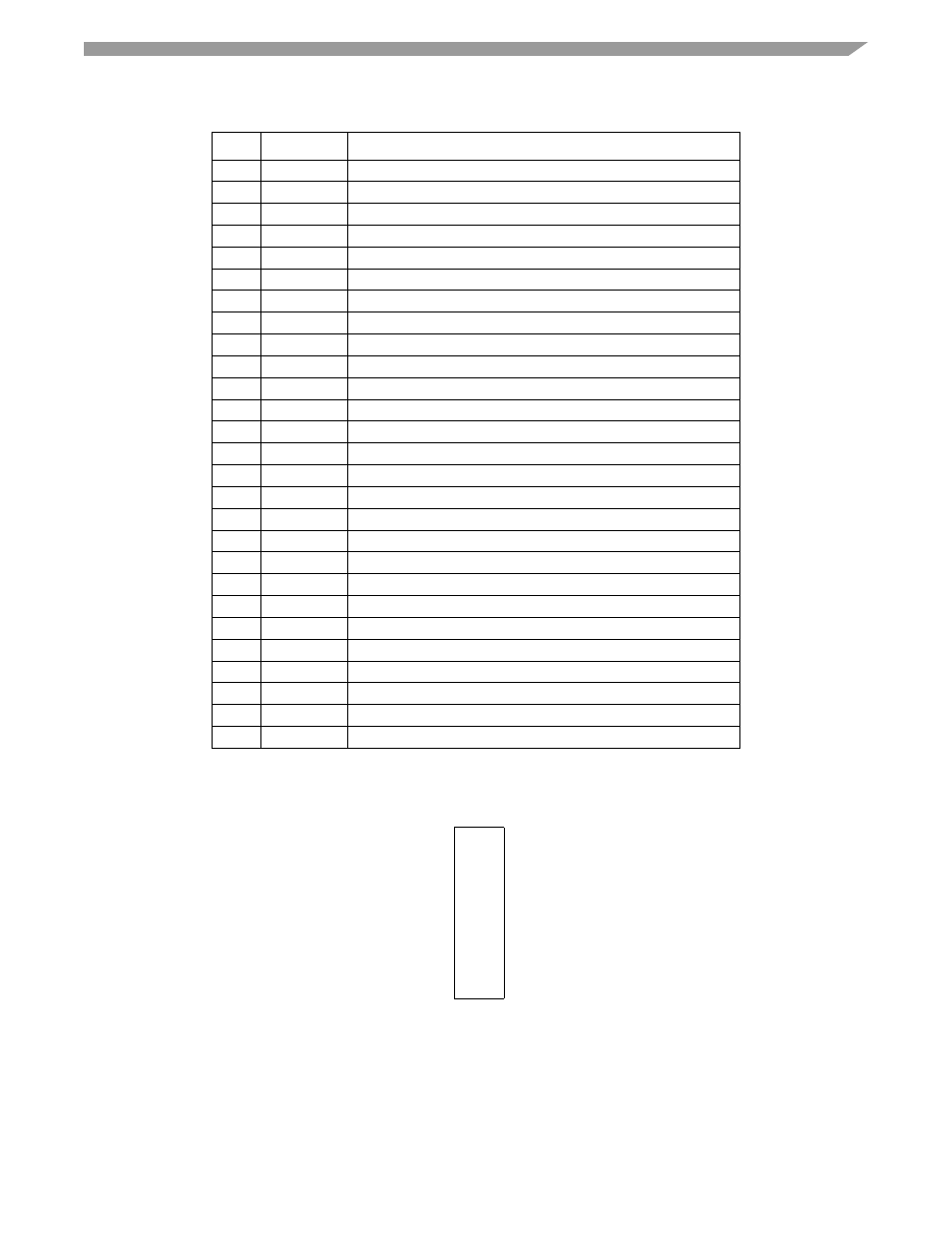
Table 3-11. NAND Flash Connector PM1 Signal Descriptions
Pin(s)
Signal
Description
1
P1.8V
+1.8 VDC power
2
NC
Not Connect
3
TP26
Test point
4
NFRB
NAND FLASH READY/BUSY
5
P2.5V
+ 2.5 VDC power
6
NFRE_B
NAND FLASH READ ENABLE
7
TP27
Test point
8
NFCE_B
NAND FLASH CHIP ENABLE
9
VCC
+3 VDC power
10
NFCLE
NAND FLASH COMMAND LATCH ENABLE
11
NC
Not Connect
12
NFALE
NAND FLASH ADDRESS LATCH ENABLE
13
NC
Not Connect
14
NFWE_B
NAND FLASH WRITE ENABLE
15
NC
Not Connect
16
NFWP_B
NAND FLASH WRITE PROTECT
17
GND
GOUND
18
GND
GOUND
19
GND
GOUND
20
GND
GOUND
23
NFIO4
NAND FLASH I/O BIT 4 — Bidirectional data transfer signal
24
A14 NFIO9 NAND FLASH I/O BIT 9 — Bidirectional data transfer signal*
25
NFIO5
NAND FLASH I/O BIT 5 — Bidirectional data transfer signal
26
A13 NFIO8 NAND FLASH I/O BIT 8 — Bidirectional data transfer signal*
27
NFIO6
NAND FLASH I/O BIT 6 — Bidirectional data transfer signal
28, 30
GND
GROUND
29
NFIO7
NAND FLASH I/O BIT 7 — Bidirectional data transfer signal
*The signal name in italics is the function intended for operation with this connector.
It is multiplexed in the i.MX21 processor with the listed signal.
PM2
NC
1
• •
2
NC
NFIO0
3
• •
4
A25
NFIO1
5
• •
6
A24
NFIO2
7
• •
8
A23
NFIO3
9
• •
10 A22
NFIO4
11
• •
12 A21
NFIO5
13
• •
14 A15
NFIO6
15
• •
16 A14
NFIO7
17
• •
18 A13
GND
19
• •
20 GND