E pk2 connector and table 3-4 provides signal – Freescale Semiconductor M9328MX21ADSE User Manual
Page 44
Support Information
M9328MX21ADSE User’s Manual, Rev. A
3-16
Freescale Semiconductor
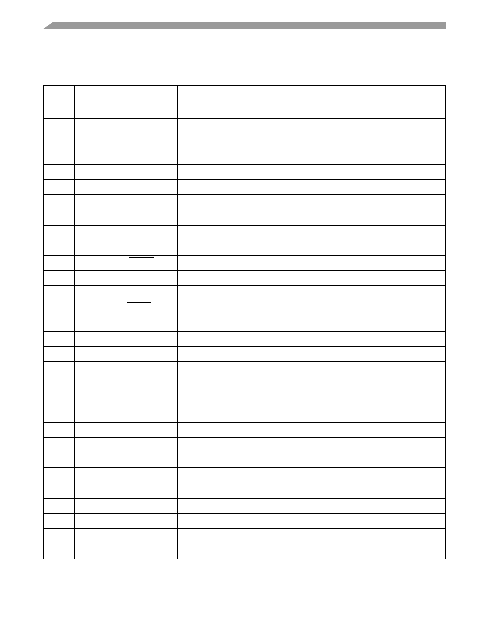
Table 3-4. CPU to Option Card PK2 Connector Signals
Pin(s)
Signal
Description
1, 60
VCC
+3.0 VDC power
2
NFIO1 PC_VS2
PCMCIA VOLTAGE SENSE 2 — Input signal to select card voltage*
3
NFIO0 PC_BVD1
PCMCIA BATTERY VOLTAGE DETECT 1 — Input signal to report battery status*
4
NFIO3 PC_WP
PCMCIA WRITE PROTECT — Input signal from the PCMCIA card*
5
NFIO2 PC_VS1
PCMCIA VOLTAGE SENSE 1 input signal to select PCMCIA card voltage*
6, 9
P2.5V
+ 2.5 VDC power
7
NFIO4 PC_READY
PCMCIA READY — Input signal to indicate the card is ready for access*
8
NFIO5 PC_WAIT
PCMCIA WAIT — Input signal to extend the current access*
10
NFIO7 PC_CD1
PCMCIA CARD DETECT 1 — Input signal to indicate a card is inserted*
11
NFIO6 PC_CD2
PCMCIA CARD DETECT 2 — Input signal to indicate a card is inserted*
12
NFRE_B PC_RW
PCMCIA READ/WRITE — Data direction control, active low to write*
13
NFWE_B PC_BVD2
PCMCIA BATTERY VOLTAGE DETECT 2 — Input signal to report battery status*
14, 53
P1.8V
+1.8 VDC power
15
NFALE PC_OE
PCMCIA OUTPUT ENABLE — Output used to enable memory read data*
16
NFCLE PC_POE
PCMCIA Buffer OUTPUT ENABLE — Output used tri-state control signals*
17
NFWP_B PC_CE2
PCMCIA CARD ENABLE 2 — Output used to enable odd bytes*
18
NFCE_B PC_CE1
PCMCIA CARD ENABLE 1 — Output used to enable even bytes*
19
NFRB PC_RST
PCMCIA RESET — Output to reset a card’s Configuration Option Register*
20
PC_PWRON
PCMCIA input to indicate card power is applied and stable
21
D23
DATA BIT 23 — Bidirectional data bit from the processor
22
D24
DATA BIT 24 — Bidirectional data bit from the processor
23
D22
DATA BIT 22 — Bidirectional data bit from the processor
24
D25
DATA BIT 25 — Bidirectional data bit from the processor
25
D21
DATA BIT 21 — Bidirectional data bit from the processor
26
D26
DATA BIT 26 — Bidirectional data bit from the processor
27
D20
DATA BIT 20 — Bidirectional data bit from the processor
28
D27
DATA BIT 27 — Bidirectional data bit from the processor
29
D19
DATA BIT 19 — Bidirectional data bit from the processor
30
D28
DATA BIT 28 — Bidirectional data bit from the processor
31
D18
DATA BIT 18 — Bidirectional data bit from the processor