Rx − 8564 lc, Absolute maximum ratings, Recommended operating conditions – Epson RX-8564LC User Manual
Page 7: Frequency characteristics

RX
−
8564
LC
Page
−
4
ETM12E-01
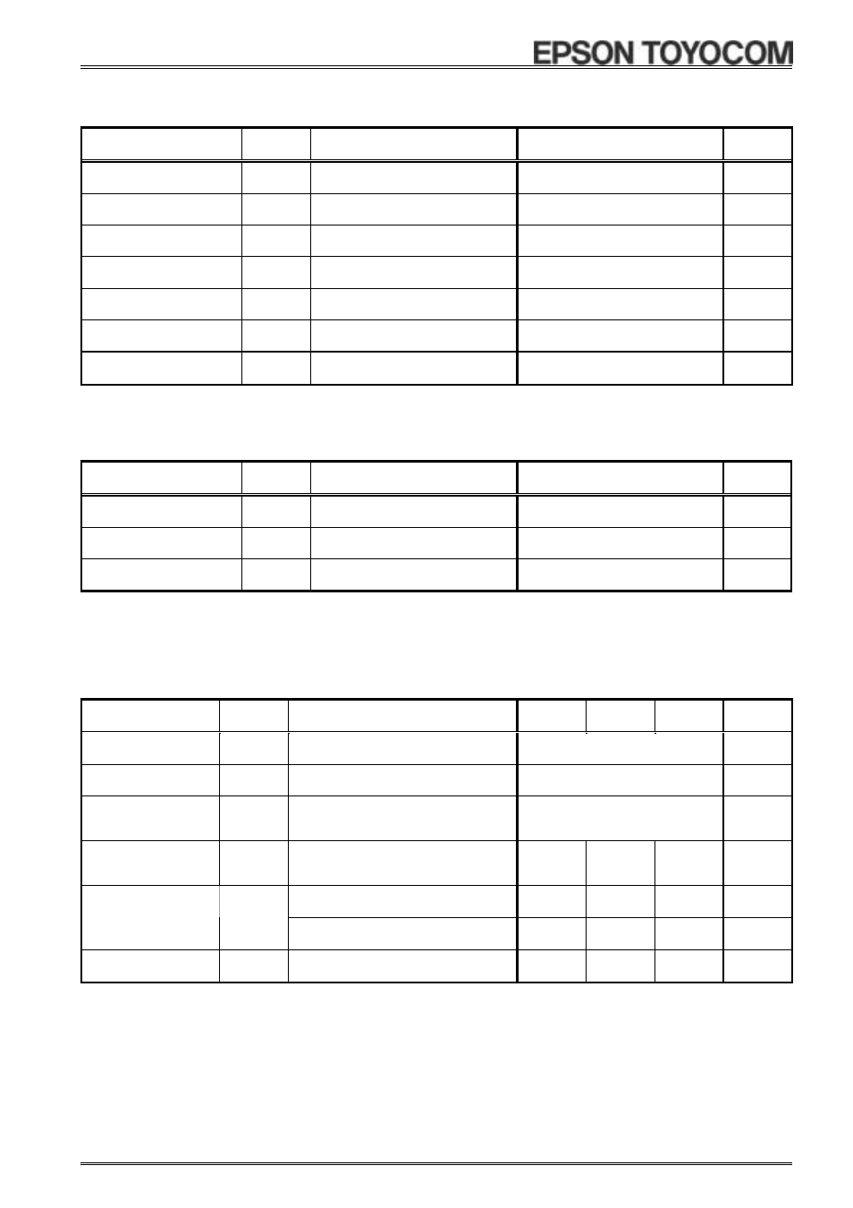
5. Absolute Maximum Ratings
GND
=
0
V
Parameter
Symbol
Condition
Rating
Unit
Supply Voltage
V
DD
Between V
DD
and GND
−
0.5 to +6.5
V
Supply Voltage
I
DD
V
DD
pin
−
50 to 50
mA
Input Voltage
V
I
Input pin
GND
−
0.5 to V
DD
+0.5
V
Output Voltage
V
O
/INT pin
GND
−
0.5 to
V
DD
+0.5
V
DC Input Current
I
I
−
10 to
10
mA
DC Output Current
I
O
−
10 to
10
mA
Storage
Temperature Range
T
STG
Stored bare product after
unpacking
−
55 to
+125
°
C
6. Recommended operating conditions
GND
=
0
V
Item
Symbol
Condition
Rating
Unit
Operating supply voltage
V
DD
I
2
C-BUS access
at 400 kHz
1.8 to 5.5
V
Clock supply voltage
V
DD
V
LOW
(
∗
1)
to 5.5
V
Operating temperature
T
OPR
No condensation
−
40 to +85
°
C
∗
1)
See "
8.1.
DC Electrical Characteristics
".
7. Frequency Characteristics
*
Unless otherwise specified, GND
=
0
V
,
Ta
=
+25
°
C
,
V
DD
=
3.0
V
Item
Symbol
Comments
Min.
Typ.
Max.
Unit
Output frequency
fo
32.768
(
Typ.
)
kHz
Frequency precision
∆
f
/
f
Ta
=
+25
°
C
V
DD
=
3.0
V
5
±
23
(
∗
1) (
∗
2)
×
10
−
6
Frequency
voltage
characteristics
f
/
V
Ta
=
+25
°
C
V
DD
=
1.8
V
to
5.5
V
±
2
(
Max.
)
×
10
−
6
/
V
Frequency
temperature
characteristics
Top
Ta
=
−
20
°
C
to
+70
°
C,
V
DD
=
3.0
V
;
Reference at +25
°
C
−
120
+10
×
10
−
6
Ta
=
+25
°
C
V
DD
=
1.8
V
3.0
s
Oscillation
startup-up time
t
STA
Ta
=
−
40
°
C
to
+85
°
C,
V
DD
=
3.0
V
3.0
s
Aging
fa
Ta
=
+25
°
C
,
V
DD
=
3.0
V
;
first year
−
5
+5
×
10
−
6
/
year
∗
1 )
This difference is 1 minute by 1 month. ( excluding offset )
∗
2 )
Includes variation in frequency during two rounds of reflow processing.
∗
Reflow processing is performed under conditions specified by Seiko Epson Corporation.
(See the relevant specifications.)
