Electrical characteristics, 1 dc electrical characteristic – ELANsat Tech OTP ROM EM78P156N User Manual
Page 38
EM78P156N
OTP ROM
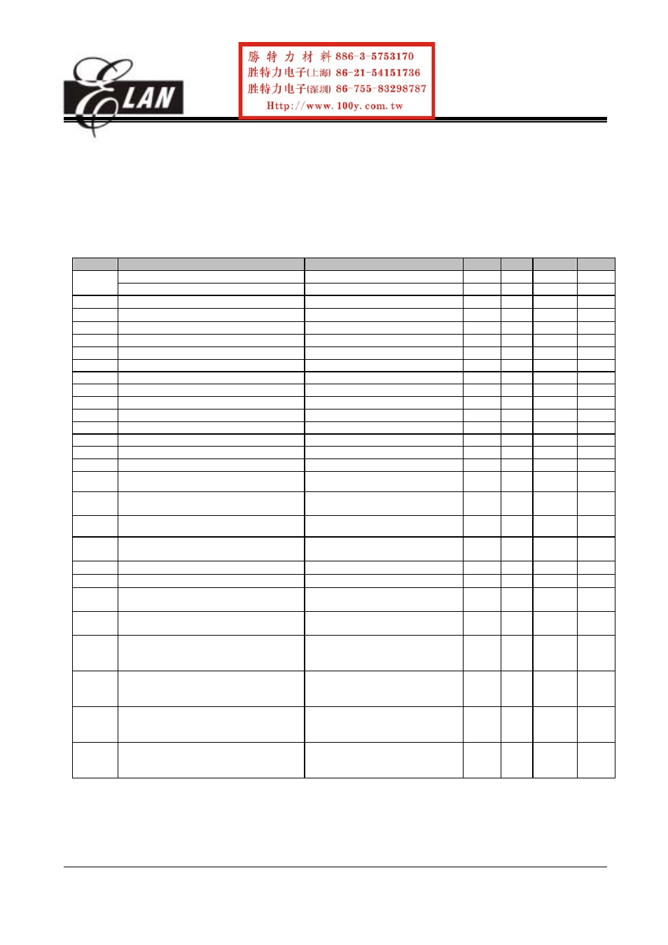
6. ELECTRICAL CHARACTERISTICS
6.1 DC Electrical Characteristic
(Ta=25
°C, VDD=5V±5%, VSS=0V)
Symbol
Parameter
Condition
Min
Typ.
Max
Unit
Two cycle with two clocks
DC
8.0
MHz
FXT
XTAL: VDD to 5V
Two cycle with two clocks
DC
20.0
MHz
ERC
ERC: VDD to 5V
R: 5.1K
Ω, C: 100 pF
F
±30% 940 F±30%
KHz
IIL
Input Leakage Current for input pins
VIN = VDD, VSS
±1
µA
VIH1
Input High Voltage (VDD=5V)
Ports 5, 6
2.0
V
VIL1
Input Low Voltage (VDD=5V)
Ports 5, 6
0.8
V
VIHT1 Input High Threshold Voltage (VDD=5V)
/RESET, TCC(Schmitt trigger)
2.0
V
VILT1
Input Low Threshold Voltage (VDD=5V)
/RESET, TCC(Schmitt trigger)
0.8
V
VIHX1
Clock Input High Voltage (VDD=5V) OSCI 3.5
V
VILX1
Clock Input Low Voltage (VDD=5V) OSCI
1.5
V
VIH2
Input High Voltage (VDD=3V)
Ports 5, 6
1.5
V
VIL2
Input Low Voltage (VDD=3V)
Ports 5, 6
0.4
V
VIHT2 Input High Threshold Voltage (VDD=3V)
/RESET, TCC(Schmitt trigger)
1.5
V
VILT2
Input Low Threshold Voltage (VDD=3V)
/RESET, TCC(Schmitt trigger)
0.4
V
VIHX2
Clock Input High Voltage (VDD=3V) OSCI 2.1
V
VILX2
Clock Input Low Voltage (VDD=3V) OSCI
0.9
V
VOH1
Output High Voltage (Ports 5)
IOH = -12.0 mA
2.4
V
VOH1
Output High Voltage (Ports 6)
(Schmitt trigger)
IOH = -12.0 mA
2.4
V
VOL1
Output Low Voltage(Port5)
IOL = 12.0 mA
0.4
V
VOL1
Output Low Voltage (Ports 6)
(Schmitt trigger)
IOL = 12.0 mA
0.4
V
IPH
Pull-high current
Pull-high active, input pin at VSS
-50
-70
-240
µA
IPD
Pull-down current
Pull-down active, input pin at VDD
25
50
120
µA
ISB
1
Power down current
All input and I/O pins at VDD,
output pin floating, WDT disabled
1 2
µA
ISB
2
Power down current
All input and I/O pins at VDD,
output pin floating, WDT enabled
15
µA
ICC1
Operating supply current
(VDD=3V)
at two cycles/four clocks
/RESET= 'High', Fosc=32KHz
(Crystal type,CLKS="0"), output
pin floating, WDT disabled
15 20 30
µA
ICC2
Operating supply current
(VDD=3V)
at two cycles/four clocks
/RESET= 'High', Fosc=32KHz
(Crystal type,CLKS="0"), output
pin floating, WDT enabled
25 35
µA
ICC3
Operating supply current
(VDD=5.0V)
at two cycles/two clocks
/RESET= 'High', Fosc=4MHz
(Crystal type, CLKS="0"), output
pin floating, WDT enabled
2.0
mA
ICC4
Operating supply current
(VDD=5.0V)
at two cycles/four clocks
/RESET= 'High', Fosc=10MHz
(Crystal type, CLKS="0"), output
pin floating, WDT enabled
4.0
mA
XTAL: VDD to 3V
* These parameters are characterizes but not tested.
This specification is subject to change without prior notice. 38
07.29.2004 (V1.2)
WW
W.100
Y.COM.TW
WW
W.100
Y.COM.TW
WW
W.100
Y.COM.TW
WW
W.100
Y.COM.TW
WW
W.100
Y.COM.TW
WW
W.100
Y.COM.TW
WW
W.100
Y.COM.TW
WW
W.100
Y.COM.TW
WW
W.100
Y.COM.TW
WW
W.100
Y.COM.TW
WW
W.100
Y.COM.TW
WW
W.100
Y.COM.TW
WW
W.100
Y.COM.TW
WW
W.100
Y.COM.TW
WW
W.100
Y.COM.TW
WW
W.100
Y.COM.TW
WW
W.100
Y.COM.TW
WW
W.100
Y.COM.TW
WW
W.100
Y.COM.TW
WW
W.100
Y.COM.TW
WW
W.100
Y.COM.TW
WW
W.100
Y.COM.TW
WW
W.100
Y.COM.TW
WW
W.100
Y.COM.TW
WW
W.100
Y.COM.TW
WW
W.100
Y.COM.TW
WW
W.100
Y.COM.TW
WW
W.100
Y.COM.TW
WW
W.100
Y.COM.TW
WW
W.100
Y.COM.TW
WW
W.100
Y.COM.TW
WW
W.100
Y.COM.TW
WW
W.100
Y.COM.TW
WW
W.100
Y.COM.TW
WW
W.100
Y.COM.TW
WW
W.100
Y.COM.TW
WW
W.100
Y.COM.TW
WW
W.100
Y.COM.TW
WW
W.100
Y.COM.TW
WW
W.100
Y.COM.TW
WW
W.100
Y.COM.TW
WW
W.100
Y.COM.TW
WW
W.100
Y.COM.TW
WW
W.100
Y.COM.TW
WW
W.100
Y.COM.TW
WW
W.100
Y.COM.TW
WW
W.100
Y.COM.TW
WW
W.100
Y.COM.TW
WW
W.100
Y.COM.TW
WW
W.100
Y.COM.TW
WW
W.100
Y.COM.TW
WW
W.100
Y.COM.TW
WW
W.100
Y.COM.TW
WW
W.100
Y.COM.TW
WW
W.100
Y.COM.TW
WW
W.100
Y.COM.TW
WW
W.100
Y.COM.TW
WW
W.100
Y.COM.TW
WW
W.100
Y.COM.TW
WW
W.100
Y.COM.TW
WW
W.100
Y.COM.TW
WW
W.100
Y.COM.TW
WW
W.100
Y.COM.TW
WW
W.100
Y.COM.TW
WW
W.100
Y.COM.TW
WW
W.100
Y.COM.TW
WW
W.100
Y.COM.TW
WW
W.100
Y.COM.TW
WW
W.100
Y.COM.TW
WW
W.100
Y.COM.TW
WW
W.100
Y.COM.TW
WW
W.100
Y.COM.TW
WW
W.100
Y.COM.TW
WW
W.100
Y.COM.TW
WW
W.100
Y.COM.TW
WW
W.100
Y.COM.TW
WW
W.100
Y.COM.TW
WW
W.100
Y.COM.TW
WW
W.100
Y.COM.TW
WW
W.100
Y.COM.TW
WW
W.100
Y.COM.TW
WW
W.100
Y.COM.TW
WW
W.100
Y.COM.TW
WW
W.100
Y.COM.TW
WW
W.100
Y.COM.TW
WW
W.100
Y.COM.TW
WW
W.100
Y.COM.TW
WW
W.100
Y.COM.TW
WW
W.100
Y.COM.TW
WW
W.100
Y.COM.TW
WW
W.100
Y.COM.TW
WW
W.100
Y.COM.TW
WW
W.100
Y.COM.TW
WW
W.100
Y.COM.TW
WW
W.100
Y.COM.TW
WW
W.100
Y.COM.TW
WW
W.100
Y.COM.TW
WW
W.100
Y.COM.TW
WW
W.100
Y.COM.TW
WW
W.100
Y.COM.TW
WW
W.100
Y.COM.TW
WW
W.100
Y.COM.TW
WW
W.100
Y.COM.TW
WW
W.100
Y.COM.TW
WW
W.100
Y.COM.TW
WW
W.100
Y.COM.TW
WW
W.100
Y.COM.TW
WW
W.100
Y.COM.TW
WW
W.100
Y.COM.TW
WW
W.100
Y.COM.TW
WW
W.100
Y.COM.TW
WW
W.100
Y.COM.TW
WW
W.100
Y.COM.TW
WW
W.100
Y.COM.TW