Avago Technologies ACPL-P340-000E User Manual
Page 2
2
1
TP_ANODE_T
TP_CATHODE_T
1
1
2
205 ohm
R1
1
2
137 ohm
R2
1
2
1
MF
50 V
C1
1
2
EC1
NM
1
2
Cbs
NM
1
2
NM
R3
1
2
NM
R4
1
2
SS32
D1
1
2
NM
Dbs
1
2
NM
Rbs
1
VCC_T
1
2
ZD1
1
2
ZD2
1
TP_OUT_T
1
2
J4
2P_HEADER
1
TP_VEE_T
1
TP_E1_T
1
2
3
NM
3P_TO220
J1
1
2
3
NM
3P_TO247
J2
1
2
3
NM
3P_HEADER
J3
G1
C1
E1
TP_G1
TP_C1
TP_E1
Anode
1
NC
2
Cathode
3
Vee
4
Vout
5
Vcc
6
U1
ACPL-P34X/W34X
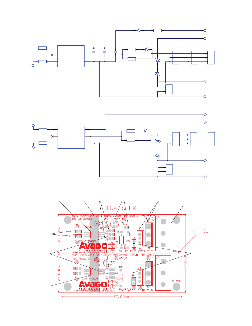
Figure 1. Schematic Diagram for ACPL-P34X/W34X Evaluation Board – Top
Figure 2. Schematic Diagram for ACPL-P34X/W34X Evaluation Board – Bottom
1
TP_ANODE_B
1
TP_CATHODE_B
1
2
205 ohm
R5
1
2
137 ohm
R6
1
2
1
MF
50 V
C2
1
2
EC2
NM
1
2
NM
R7
1
2
NM
R8
1
2
SS32
D2
1
VCC_B
1
2
ZD3
1
2
ZD4
1
TP_OUT_B
1
2
J8
2P_HEADER
1
TP_VEE_B
1
TP_E2_B
1
2
3
NM
J5
3P_TO220
1
2
3
NM
J6
3P_TO247
1
2
3
NM
J7
3P_HEADER
G2
C2
E2
TP_G2
TP_C2
TP_E2
Anode
1
NC
2
Cathode
3
Vee
4
Vout
5
Vcc
6
U2
ACPP-P34X/W34X
Isolation
Barrier
ACPL-P343/W343
Top Gate Driver
Bypass Cap
C1 & C2
Bootstrap Capacitor,
Resistor and Diode
IGBT TO-220/247
Type Package
PCB Mounting
Terminal Blocks
J3 & J7
Negative Power Supply
Jumpers J4 & J8
Split Resistors
Input LED Drive
Gate Resistors
R3, R4, R7 & R8
ACPL-P343/W343
Bottom Gate Driver
Figure 3. Top Layer View