Board connection and operation – Avago Technologies ACNT-H61L-000E User Manual
Page 3
For product information and a complete list of distributors, please go to our web site:
www.avagotech.com
Avago, Avago Technologies, and the A logo are trademarks of Avago Technologies in the United States and other countries.
Data subject to change. Copyright © 2005-2015 Avago Technologies. All rights reserved.
AV02-4757EN - January 15, 2015
DISCLAIMER: Avago’s products and software are not specifically designed, manufactured or authorized for sale
as parts, components or assemblies for the planning, construction, maintenance or direct operation of a nucle-
ar facility or for use in medical devices or applications. Customer is solely responsible, and waives all rights to
make claims against Avago or its suppliers, for all loss, damage, expense or liability in connection with such use.
Board Connection and Operation
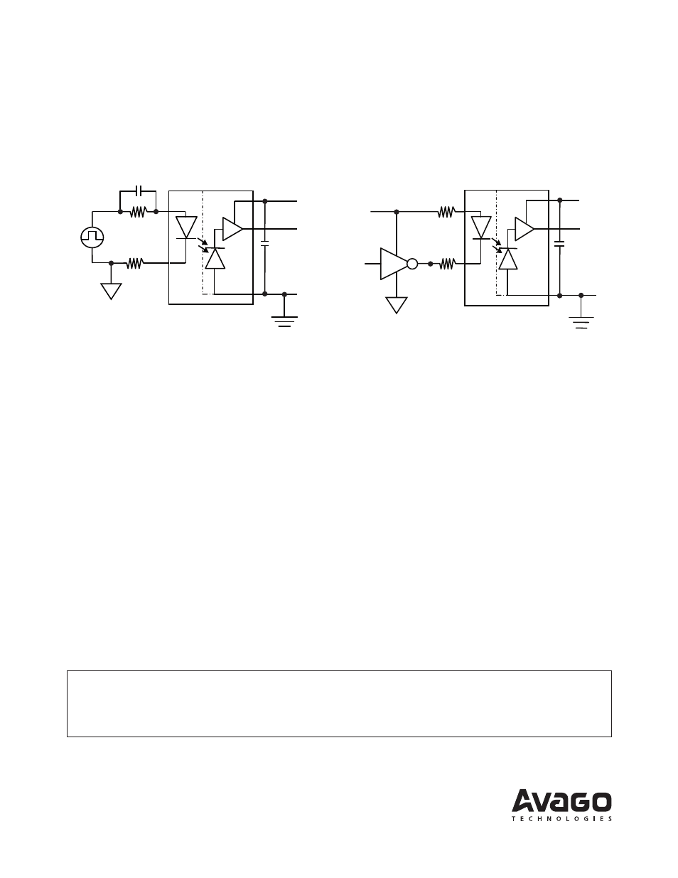
A peaking capacitor (C1–C2, C4–C5) can be placed across
the input current limit resistor (R1–R4) to achieve en-
hanced speed performance (Figure 3). The capacitance
value depends on the rise/fall time of the input signal,
supply voltages and LED input driving current. Refer to
optocoupler’s datasheet for more details.
For ACNW261L (400mil DIP8 single-channel)
1. Attach 3.3 V or 5 V pulse input signal to “ANODE1”. Input
resistors are built-in.
2. Connect input ground at “CATHODE1”.
3. Attach 3.3 V or 5 V power supply at the isolated output
side “VDD1” and “GND1”.
4. Probe the output signals at “VO1”.
Figure 3. Connection of peaking cap (Cpeak) across input resistor to improve
speed performance
Figure 4. Recommended drive circuit for high CMR
The input cathode pins connect in series to case size 1206
SMD footpath. This allows split input resistors to connect
at both anode and cathode inputs for improved CMR per-
formance (Figure 4).
For ACNT-H61L (14.2mm Stretched SO8)
1. Attach 3.3 V or 5 V pulse input signal to “ANODE2”. Input
resistors are built-in.
2. Connect input ground at “CATHODE2”.
3. Attach 3.3 V or 5 V power supply at the isolated output
side “VDD2” and “GND2”.
4. Probe the output signals at “VO2”.
GND
2
V
DD2
0.1µF
GND
1
R
1
SHIELD
V
in
+
−
C
peak
V
0
R
2
V
DD
GND
2
V
DD2
0.1µF
GND
1
R
2
R
1
Shield
V
O
74LS04 or
any totem-pole
output
logic gate