Protocol guidelines, Interference considerations, Typical applications – Linx Technologies TXM-900-HP3-xxx User Manual
Page 7
Page 13
Page 12
PROTOCOL GUIDELINES
While many RF solutions impose data formatting and balancing requirements,
Linx RF modules do not encode or packetize the signal content in any manner.
The received signal will be affected by such factors as noise, edge jitter, and
interference, but it is not purposefully manipulated or altered by the modules.
This gives the designer tremendous flexibility for protocol design and interface.
Despite this transparency and ease of use, it must be recognized that there are
distinct differences between a wired and a wireless environment. Issues such as
interference and contention must be understood and allowed for in the design
process. To learn more about protocol considerations, we suggest you read Linx
Application Note AN-00160.
Errors from interference or changing signal conditions can cause corruption of
the data packet, so it is generally wise to structure the data being sent into small
packets. This allows errors to be managed without affecting large amounts of
data. A simple checksum or CRC could be used for basic error detection. Once
an error is detected, the protocol designer may wish to simply discard the corrupt
data or implement a more sophisticated scheme to correct it.
INTERFERENCE CONSIDERATIONS
The RF spectrum is crowded and the potential for conflict with other unwanted
sources of RF is very real. While all RF products are at risk from interference, its
effects can be minimized by better understanding its characteristics.
Interference may come from internal or external sources. The first step is to
eliminate interference from noise sources on the board. This means paying
careful attention to layout, grounding, filtering, and bypassing in order to
eliminate all radiated and conducted interference paths. For many products, this
is straightforward; however, products containing components such as switching
power supplies, motors, crystals, and other potential sources of noise must be
approached with care. Comparing your own design with a Linx evaluation board
can help to determine if and at what level design-specific interference is present.
External interference can manifest itself in a variety of ways. Low-level
interference will produce noise and hashing on the output and reduce the link’s
overall range.
High-level interference is caused by nearby products sharing the same
frequency or from near-band high-power devices. It can even come from your
own products if more than one transmitter is active in the same area. It is
important to remember that only one transmitter at a time can occupy a
frequency, regardless of the coding of the transmitted signal. This type of
interference is less common than those mentioned previously, but in severe
cases it can prevent all useful function of the affected device.
Although technically it is not interference, multipath is also a factor to be
understood. Multipath is a term used to refer to the signal cancellation effects
that occur when RF waves arrive at the receiver in different phase relationships.
This effect is a particularly significant factor in interior environments where
objects provide many different signal reflection paths. Multipath cancellation
results in lowered signal levels at the receiver and, thus, shorter useful distances
for the link.
TYPICAL APPLICATIONS
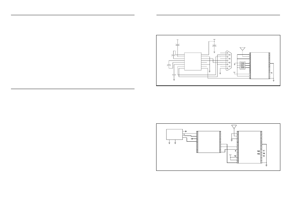
The figure below shows a typical RS-232 circuit using the HP3 Series transmitter
and a Maxim MAX232. The MAX232 converts RS-232 compliant signals to a
serial data stream, which the transmitter then sends. The MODE line is
grounded, so the channels are selected by the DIP switches.
The figure below shows a circuit using the QS Series USB module. The QS
converts USB compliant signals from a PC to serial data to be sent to the
transmitter. The MODE line is high, so the module is in Serial Channel Select
Mode. The RTS and DTR lines are used to load the channels. Application Note
AN-00155 shows sample source code that can be adapted to use on a PC. The
QS Series Data Guide and Application Note AN-00200 discuss the hardware
and software set-up required for QS Series modules.
The transmitter can also be connected to a microcontroller, which will generate
the data based on specific actions. A UART may be employed or an I / O line
may be “bit banged” to send the data to the transmitter. The transmitter may be
connected directly to the microcontroller without the need for buffering or
amplification.
Figure 14: HP3 Transmitter and MAX232 IC
C3
C4
C5
C1
C2
4.7uF
4.7uF
4.7uF
MAX232
4.7uF
DB-9
4.7uF
C1+
V+
C1-
C2+
C2-
V-
T2OUT
R2IN
R2OUT
T2IN
T1IN
R1OUT
R1IN
T1OUT
GND
VCC
VCC
GND
GND
VCC
GND
GND
1
2
3
4
5
6
7
8
9
10
11
12
13
14
15
16
1
6
2
7
3
8
4
9
5
+
+
+
+
+
VCC
GND
GND
ANT
GND
NC
NC
GND
NC
NC
NC
CS2 / SS DATA
NC
CS0
CS1 / SS CLOCK
CTS
NC
NC
1
2
3
4
5
6
7
8
17
18
19
20
21
22
23
24
PDN
VCC
MODE
NC
GND
DATA
NC
NC
9
10
11
12
13
14
16
GND
TXM-900-HP3
USB-B CONNECTOR
GND
5V
DAT -
DAT+
GND
GS
HD
GS
HD
GND
GND
1
3
4
5
6
GND
VCC
GND
SDM-USB-QS
USBDP
USBDM
GND
DSR
DATA_IN
DATA_OUT
RTS
CTS
DTR
TX_IND
VCC
SUSP_IND
RX_IND
485_TX
RI
DCD
1
2
3
4
5
6
7
8
9
10
11
12
13
14
15
16
GND
ANT
GND
NC
NC
GND
NC
NC
CS2 / SS DATA
NC
CS0
CS1 / SS CLOCK
CTS
NC
NC
1
2
3
4
5
6
7
18
19
20
21
22
23
24
PDN
VCC
MODE
NC
GND
DATA
NC
9
11
12
13
14
GND
TXM-900-HP3
Figure 15: HP3 Transmitter and Linx QS Series USB Module