Adjusting the output power, Inputting digital data, Inputting analog signals – Linx Technologies TXM-900-HP3-xxx User Manual
Page 5: Timing considerations, Transmitting data
Page 9
Page 8
ADJUSTING THE OUTPUT POWER
Depending on the type of antenna being used, the output power of the
transmitter may be higher than FCC regulations allow. It is intentionally set high
to compensate for losses resulting from inefficient antennas. Since attenuation is
often required, it is generally wise to provide for its implementation so that the
FCC test lab can easily attenuate the transmitter to the maximum legal limit.
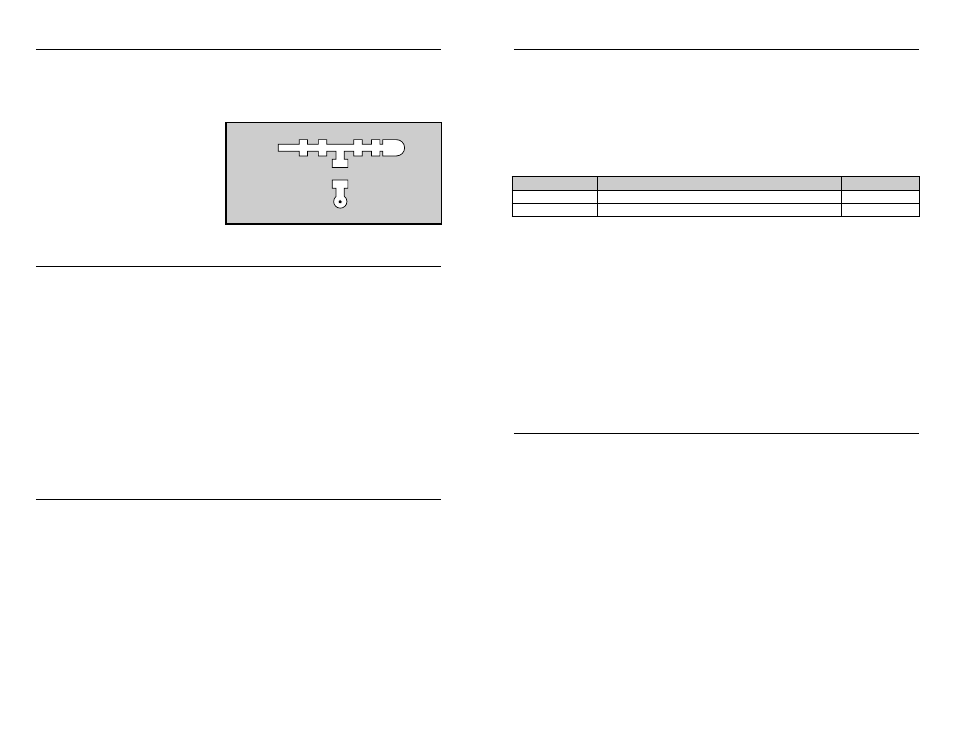
A T-pad is a network of three
resistors that allows for variable
attenuation while main taining the
correct match to the antenna. An
example layout is shown in the
adjacent figure. For more details
on T-pad attenuators, please
see Application Note AN-00150.
INPUTTING DIGITAL DATA
The DATA line may be directly connected to virtually any digital peripheral,
including microcontrollers, encoders, and UARTs. It has an impedance of 200k
Ω
and can be used with any data that transitions from 0V to a 3 to 5V peak
amplitude within the specified data rate of the module. While it is possible to send
data at higher rates, the internal filter will cause severe roll off and attenuation.
Many RF products require a fixed data rate or place tight constraints on the mark
/ space ratio of the data being sent. The HP3 transmitter architecture eliminates
such considerations and allows virtually any signal, including PWM, Manchester,
and NRZ data, to be sent at rates from 100bps to 56kbps.
The HP3 does not encode or packetize the data in any manner. This
transparency gives the designer great freedom in software and protocol
development. A designer may also find creative ways to utilize the ability of the
transmitter to accept both digital and analog signals. For example, an application
might transmit voice, then send out a digital control command. Such mixed mode
systems can greatly enhance the function and versatility of many products.
INPUTTING ANALOG SIGNALS
Analog signals from 50Hz to 28kHz may be connected directly to the
transmitter’s DATA line. The HP3 is a single supply device and, as such, is not
capable of operating in the negative voltage range. Analog sources should be
within 0 to 5V
P-P
and should, in most cases, be AC-coupled into the DATA line
to achieve the best performance. The size of the coupling capacitor should be
large enough to ensure the passage of all desired frequencies and small enough
to allow the start-up time desired. Since the modulation voltage applied to the
DATA line determines the carrier deviation, distortion can occur if the DATA line
is over-driven. The actual level of the input waveform should be adjusted to
achieve optimum in-circuit results for your application.
The HP3 is capable of providing audio quality comparable to a radio or intercom.
In applications where higher quality audio is required, a compandor may be
employed to increase dynamic range and reduce noise. If true high-fidelity audio
is required, the HP3 is probably not the best choice, as it is optimized for data.
TIMING CONSIDERATIONS
Timing plays a key role in link reliability, especially when the modules are being
rapidly turned on and off or hopping channels. Unlike a wire, allowance must be
made for the programming and settling times of both the transmitter and
receiver, or portions of the signal will be lost. There are two major timing
considerations the engineer must consider when designing with the HP3 Series
transmitter. These are shown in the table below. The stated timing parameters
assume a stable supply of 2.8 volts or greater. They do not include the charging
times of external capacitance on the module’s supply lines, the overhead of
external software execution, or power supply rise times.
T1 is the maximum time required for the transmitter to power-up and lock on-
channel. This time is measured from the application of V
CC
to the CTS line
transitioning high.
T2 is the worst-case time needed for a powered-up module to switch between
channels after a valid channel selection. This time does not include external
overhead for loading a desired channel in Serial Channel Select Mode.
Normally, the transmitter will be turned off after each transmission. This is
courteous use of the airwaves and reduces power consumption. The transmitter
may be shut down by switching its supply or the PDN line. When the transmitter
is again powered up, allowance must be made for the requirements above.
In many cases, the transmitter will lock more quickly than the times indicated.
When turn-around time or power consumption are critical, the CTS line can be
monitored so data may be sent immediately upon transmitter readiness.
TRANSMITTING DATA
Once an RF link has been established, the challenge becomes how to effectively
transfer data across it. While a properly designed RF link provides reliable data
transfer under most conditions, there are still distinct differences from a wired link
that must be addressed. Since the modules do not incorporate internal encoding
or decoding, the user has tremendous flexibility in how data is handled.
It is important to separate the types of transmissions that are technically possible
from those that are legally allowed in the country of operation. Application Notes
AN-00126, AN-00140 and Part 15, Section 249 of the FCC rules should be
reviewed for details on acceptable transmission content in the U.S.
If you want to transfer simple control or status signals (such as button presses)
and your product does not have a microprocessor or you wish to avoid protocol
development, consider using an encoder / decoder IC set. These chips are
available from several manufacturers, including Linx. They take care of all
encoding and decoding functions and provide a number of data lines to which
switches can be directly connected. Address bits are usually provided for
security and to allow the addressing of multiple receivers independently. These
ICs are an excellent way to bring basic remote control products to market quickly
and inexpensively. It is also a simple task to interface with inexpensive
microprocessors or one of many IR, remote control, DTMF, or modem ICs.
Parameter
Description
Max.
T1
Transmitter turn-on time
10.0mS
T2
Channel change time (time to valid data)
1.5mS
GROUND PLANE
ON LOWER LAYER
ANTENNA
RF
MODULE
R1
R1
R2
GROUND
Figure 12: T-Pad Attenuator Example Layout