Caution, Typical performance graphs, Absolute maximum ratings – Linx Technologies TXM-900-HP3-xxx User Manual
Page 2: Electrical specifications, Performance data
Page 3
Page 2
1
2
CH1 1.00V
Delta 7.200mS
2.5mS
CH2 2.00V
VCC / PDN
CTS
Figure 3: Power-up to CTS
TYPICAL PERFORMANCE GRAPHS
CH1 2.00V
250
μS
CH2 500mV
IN
OUT
Figure 6: Square Wave Modulation Linearity
Figure 5: Sine Wave Modulation Linearity
CH1 2.00V
250
μS
CH2 500mV
IN
OUT
CH1 1.00V
1
Delta 7.200mS
2.5mS
2
CH2 2.00V
VCC / PDN
RX DATA
Figure 4: TX Power-up to Valid RX Data
ABSOLUTE MAXIMUM RATINGS
Supply Voltage V
CC
-0.3
to
+18.0
VDC
Any Input or Output Pin
-0.3
to
V
CC
VDC
Operating Temperature
-30
to
+85
°C
Storage Temperature
-45
to
+85
°C
Soldering Temperature
+260°C for 10 seconds
*NOTE*
Exceeding any of the limits of this section may lead to permanent
damage to the device. Furthermore, extended operation at these maximum
ratings may reduce the life of this device.
ELECTRICAL SPECIFICATIONS
Parameter
Designation
Min.
Typical
Max.
Units
Notes
POWER SUPPLY
Operating Voltage
V
CC
2.8
3.0
13.0
VDC
–
Supply Current
I
CC
–
14.0
17.0
mA
1
Power-Down Current
I
PDN
–
–
15.0
µA
2
TRANSMIT SECTION
Transmit Frequency Range
F
C
902.62
–
927.62
MHz
3
Center Frequency Accuracy
–
-50
–
+50
kHz
–
Available Channels
–
8 (Par.)
–
100 (Ser.)
–
4
Channel Spacing
–
–
250
–
kHz
–
Occupied Bandwidth
–
–
115
140
kHz
–
Output Power
P
O
-3
0
+3
dBm
5
Spurious Emissions
–
–
-45
–
dBm
6
Harmonic Emissions
P
H
–
-60
-47
dBm
6
Data Rate
–
100
–
56,000
bps
7
Analog / Audio Bandwidth
–
50
–
28,000
Hz
7
Data Input:
Logic Low
–
0.0
–
0.5
VDC
–
Logic High
–
2.8
–
5.2
VDC
–
Data Input Impedance
–
–
200
–
k
Ω
–
Frequency Deviation @ 3VDC
–
60
70
110
kHz
8
Frequency Deviation @ 5VDC
–
90
115
140
kHz
8
ANTENNA PORT
RF Output Impedance
R
OUT
–
50
–
Ω
–
TIMING
Transmitter Turn-On Time
–
–
7.0
10.0
mSec
–
Channel Change Time
–
–
1.0
1.5
mSec
–
ENVIRONMENTAL
Operating Temperature Range
–
-30
–
+85
°
C
–
1. Over the entire operating voltage range.
2. With the PDN pin low.
3. Serial
Mode.
4. 100 serial channels on the PS versions only.
5. Does not change over the 3-13VDC supply.
6. Into 50 ohms.
7. The receiver will not reliably hold a DC level. See the HP3 Series Receiver Module Data Guide for the
minimum transition rate.
8. The voltage specified is the modulation pin voltage.
Notes
*CAUTION*
This product incorporates numerous static-sensitive components.
Always wear an ESD wrist strap and observe proper ESD handling
procedures when working with this device. Failure to observe this
precaution may result in module damage or failure.
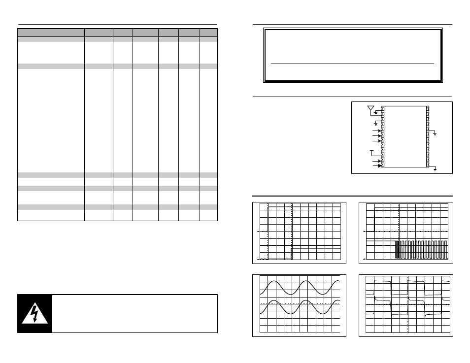
PERFORMANCE DATA
These performance parameters
are based on module operation at
25°C from a 5.0VDC supply unless
otherwise noted. Figure 2
illustrates the connections
necessary for testing and
operation. It is recommended all
ground pins be connected to the
ground plane. The pins marked NC
have no electrical connection.
Figure 2: Test / Basic Application Circuit
GND
ANT
GND
NC
NC
GND
NC
NC
NC
CS2 / SS D
NC
CS0
CS1 / SS CLOCK
CTS
NC
NC
PDN
VCC
MODE
NC
GND
DATA
NC
NC
5VDC
PC
PC
PC
PC
Table 1: HP3 Series Transmitter Specifications