Chapter 3, Board layout, Connectors and jumpers list – Lanner LEC-2530 User Manual
Page 13
13
Board Layout
Chapter 3
Embedded and Industrial Computing
Connectors and Jumpers List
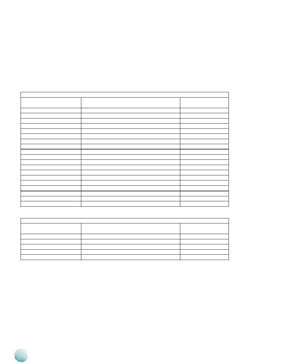
The tables below list the function of each of the board
jumpers and connectors by labels shown in the above
section. The next section in this chapter gives pin
definitions and instructions on setting jumpers.
Table 3.1 Connector List for LEB-2530 Board
Labels
Function
Pin Definition Refer-
ence Page
CF1
CompactFlash Connector
P16
COM1/COM2
RS232 Serial Ports COM1 and COM2
P14
DIO1
Digital Input/Output
P16
HDMI1
High-Definition Multimedia Interface Port
P15
JCMOS1
Clear CMOS Jumper
P15
JCOM1/2
RS232 Pin Headers
P14
JKBMS1
PS/2 Keyboard & Mouse Connector
P16
JLPC1
Low-pin Count Interface
Reserved for Factory Use
JRI1/2
COM1/COM2 Pin 9 Signal Selection
P14
JSPI1
SPI ROM Interface (for debug use only)
Reserved for Factory Use
LAN1/LAN2
RJ45 Ethernet Ports
P15
MPCIE1
Mini-PCIe Connectors (with SIM1)
P16
PSBTN2
Power Button with Phoenix Connector
P16
SATA1
Serial-ATA Connector (SATA1)
P15
SATAPWR1
SATA HDD Power Connector
P15
SIM1
SIM Card Reader
P16
USB1
USB 2.0 Type A Dual Port
P15
USB2
USB 3.0 Type A Port
P15
VGA1
VGA Connector
P15
Table 3.2 Connector List for LEK-IOA10 Board
Labels
Function
Pin Definition Refer-
ence Page
COM3/COM4
RS232 Serial Ports COM3 and COM4
P17
USB1
USB 2.0 Type A Dual Port
P17
MPCIE1
Mini-PCIe Connectors (with SIM1)
P17
DCIN1
DC-IN Connector
P17
USB_SEL1
USB Signal Selection
P17