Chapter 3, Board layout – Lanner LEC-2055 User Manual
Page 14
14
Board Layout
Chapter 3
Embedded and Industrial Computing
Pin No.
Pin Name
Pin No.
Pin Name
7
CE1#
32
CE3#
8
GND
33
VS1
9
GND
34
IOR#
10
GND
35
IOW#
11
GND
36
WE#
12
GND
37
IDEIRQ
13
VCC3
38
VCC3
14
GND
39
CBSEL#
15
GND
40
VS2
16
GND
41
RESET#
17
GND
42
IORDY
18
A2
43
DREG
19
A1
44
DACK#
20
A0
45
ACTLED#
21
DATA0
46
BVD1
22
DATA1
47
DATA8
23
DATA2
48
DATA9
24
IOS16
49
DATA10
25
CD2-
50
GND
Dual USB Port Connector 0 and 1 (USB1):
USB 2.0 Pin Header (USBB1):
PS/2 Keyboard & Mouse Connector (KM1):
LAN Ports (LANB1/LANB2):
Pin No.
Description
Fast Ethernet Gigabit Ethernet
1
TX+
BI_DA+
2
TX-
BI_DA-
3
RX+
BI_DB+
4
--
BI_DC+
5
--
BI_DC-
6
RX-
BI_DB-
7
--
BI_DD+
8
--
BI_DD-
Clear CMOS jumper (CCMOS1): It is for clearing the
CMOS memory.
VGA Interface Cable Connector (VGA1): It is used for
connecting a VGA monitor.
Antenna Power Connector (ATNC1): It supplies power to
the wireless signal amplifier, if there is one attached to the
system.
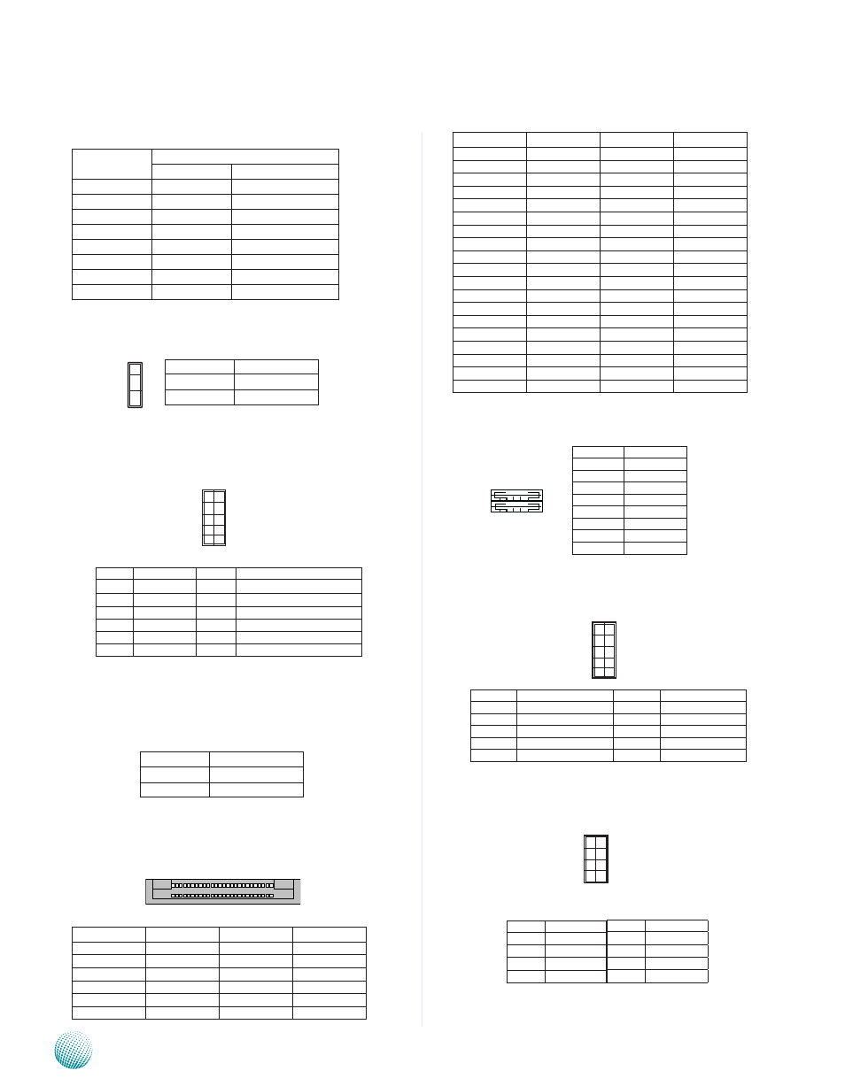
CompactFlash Connector (CF1): It is for connecting a
Compact Flash card to be served as your system’s storage.
Pin No.
Pin Name
Pin No.
Pin Name
1
GND
26
CD1-
2
DATA3
27
DATA11
3
DATA4
28
DATA12
4
DATA5
29
DATA13
5
DATA6
30
DATA14
6
DATA7
31
DATA15
Pin No.
Pin Name
1-2
Normal (Default)
2-3
Clear CMOS
25 1
50 26
Pin No.
Pin Name
1
+5V
2
USB1-
3
USB1+
4
GND
5
+5V
6
USB0-
7
USB0+
8
GND
Pin No.
Pin Name
Pin No.
Pin Name
1
+5V
2
GND
3
KEY
4
USB3+
5
USB2-
6
USB3-
7
USB2+
8
KEY
9
GND
10
+5V
1 2 3 4
5 6 7 8
Pin No. Pin Name
1
+5V
3
MSDATA
5
KBDATA
7
GND
Pin No. Pin Name
2
MSCLK
4
KEY
6
KEY
8
KBCLK
1
3
5
7
9
2
4
6
8
10
1
3
5
7
2
4
6
8
1
2
3
12
2
11
1
Pin No. Pin Name
Pin No.
Pin Name
1
R
2
Detect VGA Plug on
3
G
4
Ground
5
B
6
Ground
7
H-SYNC
8
Ground
9
V-SYNC
10
Ground
11
I2C Data
12
I2C CLOCK
Pin No.
Pin Name
1
+3.3V
2
GND