Chapter 3, Board layout – Lanner VES-8X2 User Manual
Page 13
13
Board Layout
Chapter 3
Embedded and Industrial Computing
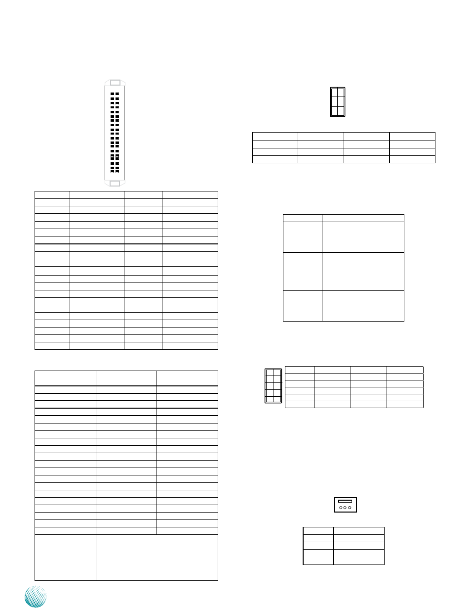
TV Out Connector (JTV1)
Pin No.
Description
Pin No.
Description
1
Pb
2
GND
3
Y
4
C
5
GND
6
GND
Signal Description for JTV1:
Signal
Description
Pb
TVDAC Channel A Output:
supports CVBS signal of
Composite; Chrominance (Pb)
analog signal of Component.
Pr
TVDAC Channel B Output:
supports Chrominance analog
signal of S-Video; Chromi-
nance (Pr) analog signal of
Component.
Y
TVDAC Channel C Output:
supports Luminance signal of
S-Video; Luminance (Y) ana-
log signal of Component.
USB Connector 7, 4 & 5 (JUSB1, JUSB2)
CPU Fan connector/ System Fan connector 1/ System
Fan connector 2
(C_FAN1/ S_FAN1/ S_FAN2)
Pin
Signal
1
GND
2
+12V
3
FANIO2/ FANIO3/
FANIO1
LVDS Connector (JLVDS1)
PIN
Pin Name
PIN
Pin Name
1
LVDS_+3.3V
2
LVDS_+5V
3
LVDS_+3.3V
4
LVDS_+5V
5
I
2
C_CLK
6
I
2
C_DAT
7
GND
8
GND
9
LCDDO3
10
LCDDO1
11
LCDDO2
12
LCDDO0
13
GND
14
GND
15
LCDDO9
16
LCDDO5
17
LCDDO8
18
LCDDO4
19
GND
20
GND
21
LCDDO13
22
LCDDO11
23
LCDDP12
24
LCDDO10
25
GND
26
GND
27
LCDDO19
28
LCDDO15
29
LCDDO18
30
LCDDO14
31
GND
32
GND
33
LCDDO17
34
LCDDO7
35
LCDDO16
36
LCDDO6
37
GND
38
GND
39
+12V_LVDS
40
+12V_LVDS
Signal Description for JLVDS1
Signal
1 Pixel / Clock LVDS
Mode
2 Pixel / Clock LVDS
Mode
LCDDO0
Txout0#
Odd Txout0#
LCDDO1
Txout0
Odd Txout0
LCDDO2
Txout1#
Odd Txout1#
LCDDO3
Txout1
Odd Txout1
LCDDO4
Txout2#
Odd Txout2#
LCDDO5
Txout2
Odd Txout2
LCDDO6
Txclk#
Odd Txclk#
LCDDO7
Txclk
Odd Txclk
LCDDO8
Txout3#
Odd Txout3#
LCDDO9
Txout3
Odd Txout3
LCDDO10
-
Even Txout0#
LCDDO11
-
Even Txout0
LCDDO12
-
Even Txout1#
LCDDO13
-
Even Txout1
LCDDO14
-
Even Txout2#
LCDDO15
-
Even Txout2
LCDDO16
-
Even Txclk#
LCDDO17
-
Even Txclk
LCDDO18
-
Even Txout3#
LCDDO19
-
Even Txout3
I2C_DAT, I2C_CLK I
2
C interface for panel parameter EEPROM.
This EERPOM is mounted on the LVDS
receiver. The data in the EEPROM allows the
COM Express module to automatically set the
proper timing parameters for a specific LCD
panel.
1
2
3
Pin No.
Pin Name
Pin No.
Pin Name
1
+5V
2
GND
3
D6-/D4-
4
GND
5
D6+/D4+
6
D7+/D5+
7
GND
8
D7-/D5-
9
GND
10
+5V
1
3
9
3 2 1
39
1