Chapter 3, Motherboard information – Lanner FW-8895 User Manual
Page 19
15
Motherboard Information
Chapter 3
Network Application Platforms
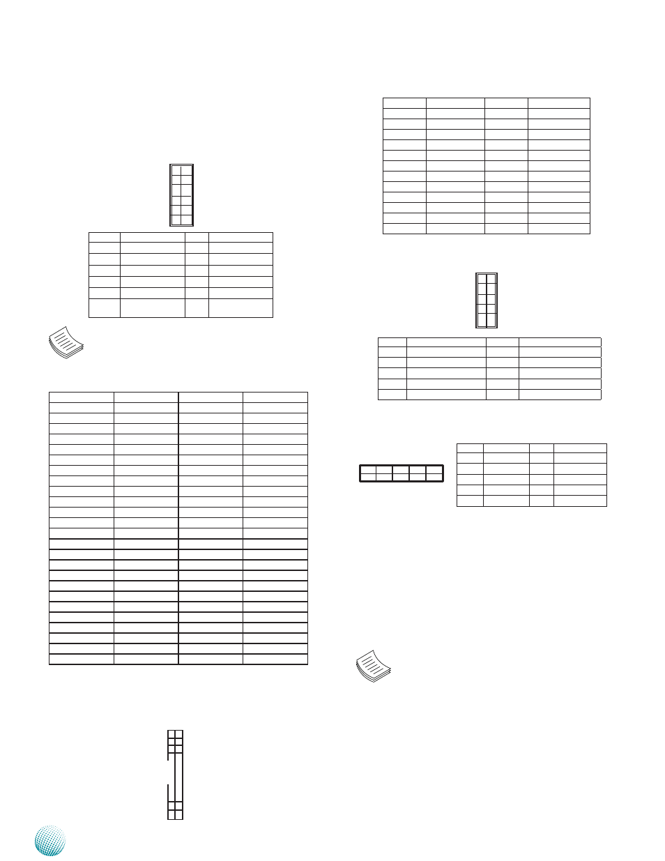
PIN
DESCRIPTION
PIN
DESCRIPTION
1
VCC
2
IOGND
3
LSTIN-
4
VEE
5
LAFD-
6
LINIT-
7
LPD1
8
LPD0
9
LPD3
10
LPD2
11
LPD5
12
LPD4
13
LPD7
14
LPD6
15
LCD
16
VCC
17
K1
18
K2
19
K3
20
K4
21
RESET
22
VCC3
23
GPIO
24
VCC3
COMA1: COM PORT Connector
COMB1: COM PORT
DIMM Sockets:
Since the system is capable of Quad Channel
configuration, some installation guidelines have to be
followed to enable Quad Channel mode. To insert 4
DIMMs on the system, insert DIMMS into the 4 slots with
black latches nearest to the designated CPU socket (CPU
socket No1 or No2). And then use slots with white latches
if more slots are required.
Note:
1.
To activate Dual Channel instead of Quad
Channel in the system, populate any 2 slots
with black latches nearest to the designated
CPU socket (CPU socket No1 or No2). And then
use slot with white latch that belongs to the
same channel as the populated slot with black
latch for any additional DIMMs.
2.
Starting from the board edge (same for both
CPU socket No1 and No2), one pair of black
and white-latched slots is configured as one
channel.
VGA1: VGA Interface. with a 2x6 (2.54”) pin header.
It is for connecting the VGA interface cable. Note the
IPMI card (connector Reference NO. OPMA1) has to be
present for this connector to work, i.e., the IPMI card
provides VGA interface/signal.
Note: A 2x6 pin (2.0”) header (J1) on the OPMA card
is also provided as an VGA interface connector.
CF1: CF Card Connector
Pin No.
Description
Pin No.
Description
1
GND
26
CD1-
2
DATA3
27
DATA11
3
DATA4
28
DATA12
4
DATA5
29
DATA13
5
DATA6
30
DATA14
6
DATA7
31
DATA15
7
CE1#
32
CE2#
8
A10
33
VS1#
9
OE#
34
IOR#
10
A9
35
IOW#
11
A8
36
WE#
12
A7
37
READY#
13
CFVCC3
38
CFVCC3
14
A6
39
CSEL
15
A5
40
VS2#
16
A4
41
RESET
17
A3
42
WAIT#
18
A2
43
INPACK#
19
A1
44
REG#
20
A0
45
DASP#
21
DATA0
46
DIAG#
22
DATA1
47
DATA8
23
DATA2
48
DATA9
24
WP
49
DATA10
25
CD2-
50
GND
J23: Parallel -type front LCM connector. It supports
both text and graphic type of LCM. The board also
facilitates USB -type LCM connector, refer to jumper
LCM_1.
9
7
5
3
1
10
8
6
4
2
1
3
5
23
2
4
6
24
Pin No.
Description
Pin No.
Description
1
DCD1
2
DSR1
3
RXD1
4
RTS1
5
TXD1
6
CTS1
7
DTR1
8
RI1
GND
10
FP_RESET_N
9 7 5 3 1
1 0 8 6 4 2
Pin No.
Description
Pin No.
Description
1
DCD2-
2
DSR2-
3
RXD2
4
RTS2-
5
TXD2
6
CTS2-
7
DTR2-
8
RI2-
9
GND
10
Pin No.
Function
Pin No
Function
1
R
2
Ground
3
G
4
Ground
5
B
6
Ground
7
H-SYNC
8
Ground
9
V-SYNC
10
Ground
11
Detect-display
Data
12
Deteck-display
CLOCK
11
9
7
5
3
1
12
10
8
6
4
2