Sundance FC203B User Manual
Page 5
Page 5 of 5
Revision 0.5
Sundance Digital Signal Processing Inc.
4790 Caughlin Parkway 233, Reno, NV 89519-0907, U.S.A.
Tel: +1 (775) 827-3103, Fax: +1 (775) 827-3664, email:
www.sundancedsp.com
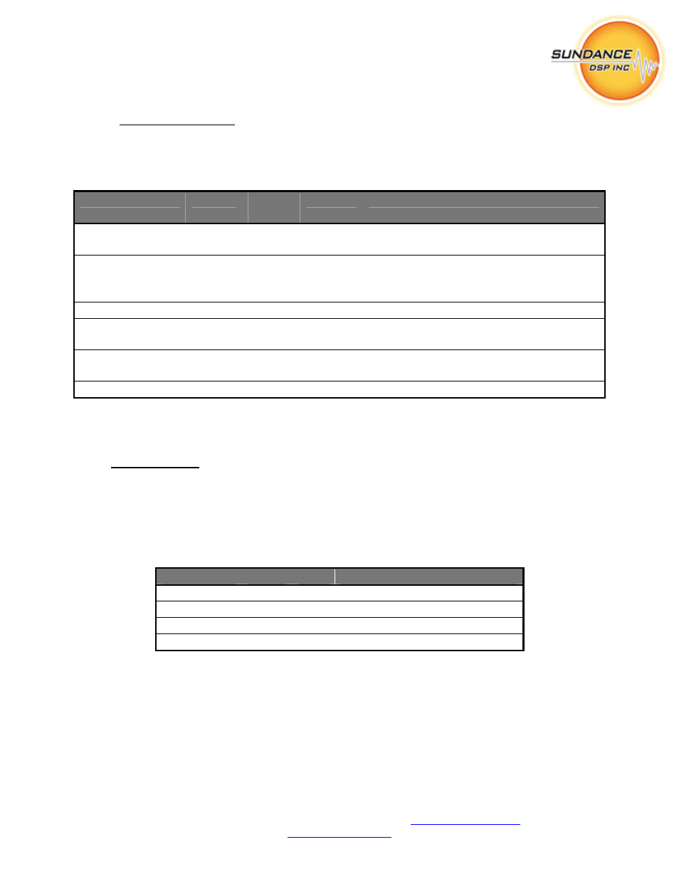
2. I/O
DESCRIPTION
The FC203B component presents as a pure-FPGA ‘task’, and implements the following
interface:
Port Name
Channel Valid
Width
Direction
Description
FMDA_CM_IN
0
20
Input
Encodes the number of frequency bins and
channels implemented in FDMA_IN
F0_IN..F3_IN 1..4 64 Input In-Phase/Quadrature
components,
frequency domain data, two channels per
link
CTRL_IN 5
32
Input
Control
Word
FDMA_OUT
0
32
Output
Frequency domain multiple access
(highway output)
FDMA_CM_OUT 1
20
Output
Encodes the number of frequency bins and
channels implemented in FDMA_OUT
STATUS_OUT 2
32
Output Pass-through
control/status
Table 1 –FC203B Interfaces
Additional port descriptions are provided below:
FDMA_CM_IN
This port drives the current configuration of the FDMA_OUT port, as described below. Bits
0...12 represent the number of frequency bins, M (up to 4096) while bits 16...19 represent the
number of channels that are interleaved, C. A ‘C’ value of zero will create 16 channels in the
FDMA_highway, although this module is only capable of filling up to 8. This port is suitable for
connecting to any FDMA_CM_OUT port.
Signal
Bits
Mode Description
M
12..lsb R/W
Number of samples per frame
RESERVED 15..13 R/W Pass-through
(reserved)
C
19..16 R/W
Number of active channels
RESERVED 31..20 R/W Pass-through
(reserved)
Table 2 – Format of FDMA_CM_IN control word
NOTE: To simplify the FPGA logic, the control word is assumed to be static while the module is
enabled. Changes to M or C while any ENABLE bit is set will result in unpredictable output.
NOTE: C=1 is currently not supported.