8 gpio (general purpose i/o), Gpio (general purpose i/o) – Sundance SMT362 User Manual
Page 13
4.2.8 GPIO (General Purpose I/O)
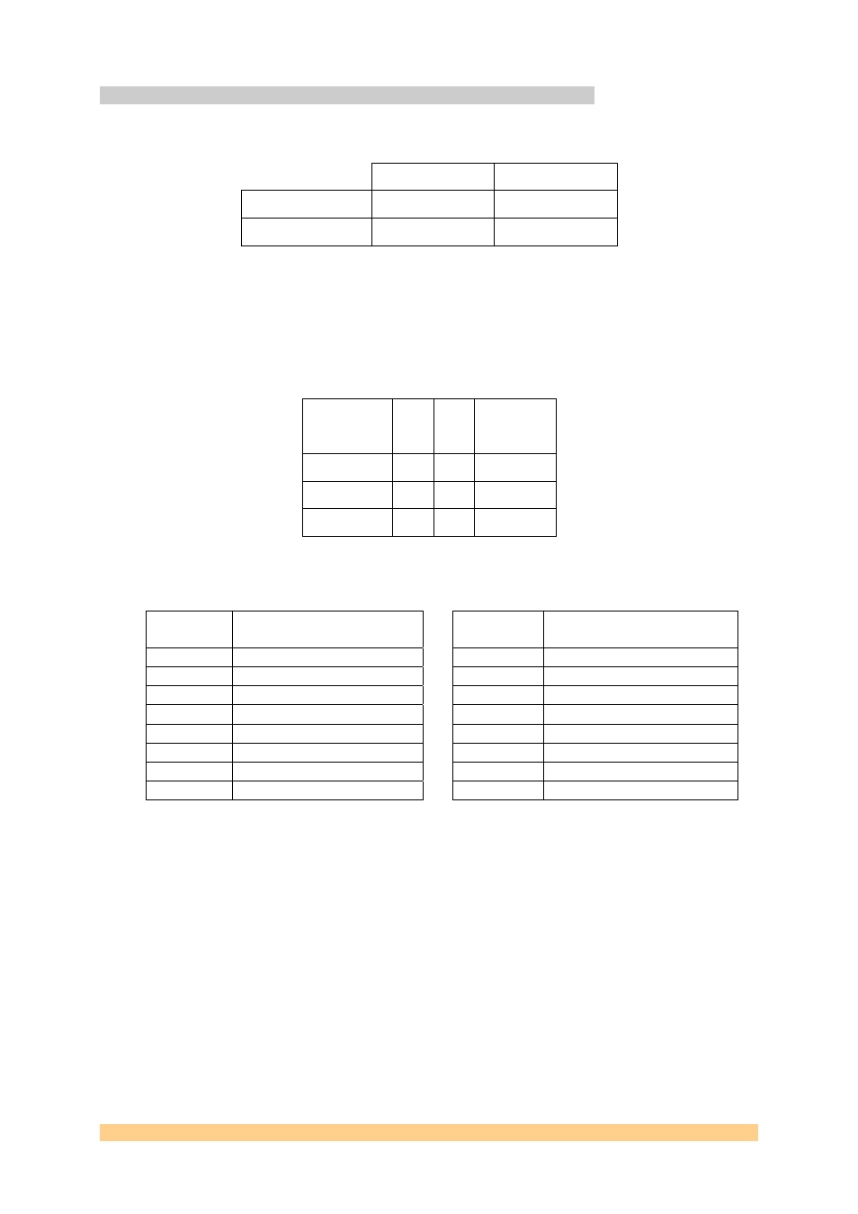
Two GPIO signals from each DSP are used to illuminate LEDs as shown here;
DSPA
DSPB
GPIO 14
D3
D5
GPIO 15
D2
D4
The LEDs are labelled on the board as ‘Dn’.
Four other GPIO signals from the FPGA are connected directly (un-buffered, 3.3V LVTTL
ONLY) to connector JP3. The pin-out and FPGA pad number is shown here;
Signal Pin Pin
Signal
3.3V 1
4
Pad
D10
Ground 2 5 Pad
H10
Pad C10
3
6
Pad G10
All of the DSP’s GPIO signals are described here;
GPIO Function
GPIO Function
0
CLKR1 (to FPGA)
8
DR1 (to FPGA)
1
SYSCLK3
9
DX1 (to FPGA)
2
PROG
10
FSR1 (to FPGA)
3
CLKX1 (to FPGA)
11
FSX1 (to FPGA)
4
INT4 (to FPGA)
12
Flash A20
5
INT5 (to FPGA)
13
Flash A21
6
INT6 (to FPGA)
14
LED1
7
INT7 (to FPGA)
15
LED2
The McBSP signals (CLKR1, CLKX1, DR1, DX1, FSR1 and FSX1) are all connected to the
FPGA. They are normally set to function as McBSP signals, but it is possible to enable these
as GPIO and hence a source of a further 6 interrupts to the DSP.
The above signals are independent between DSPs.
GPIO2, 12 and 13 are connected to the FPGA on DSPB (DSPB does not have access to a
flash memory and cannot configure the FPGA).
User Manual SMT362
Page 13 of 30
Last Edited: 29/04/2009 08:56