Architecture description – Sundance SMT338-VP User Manual
Page 6
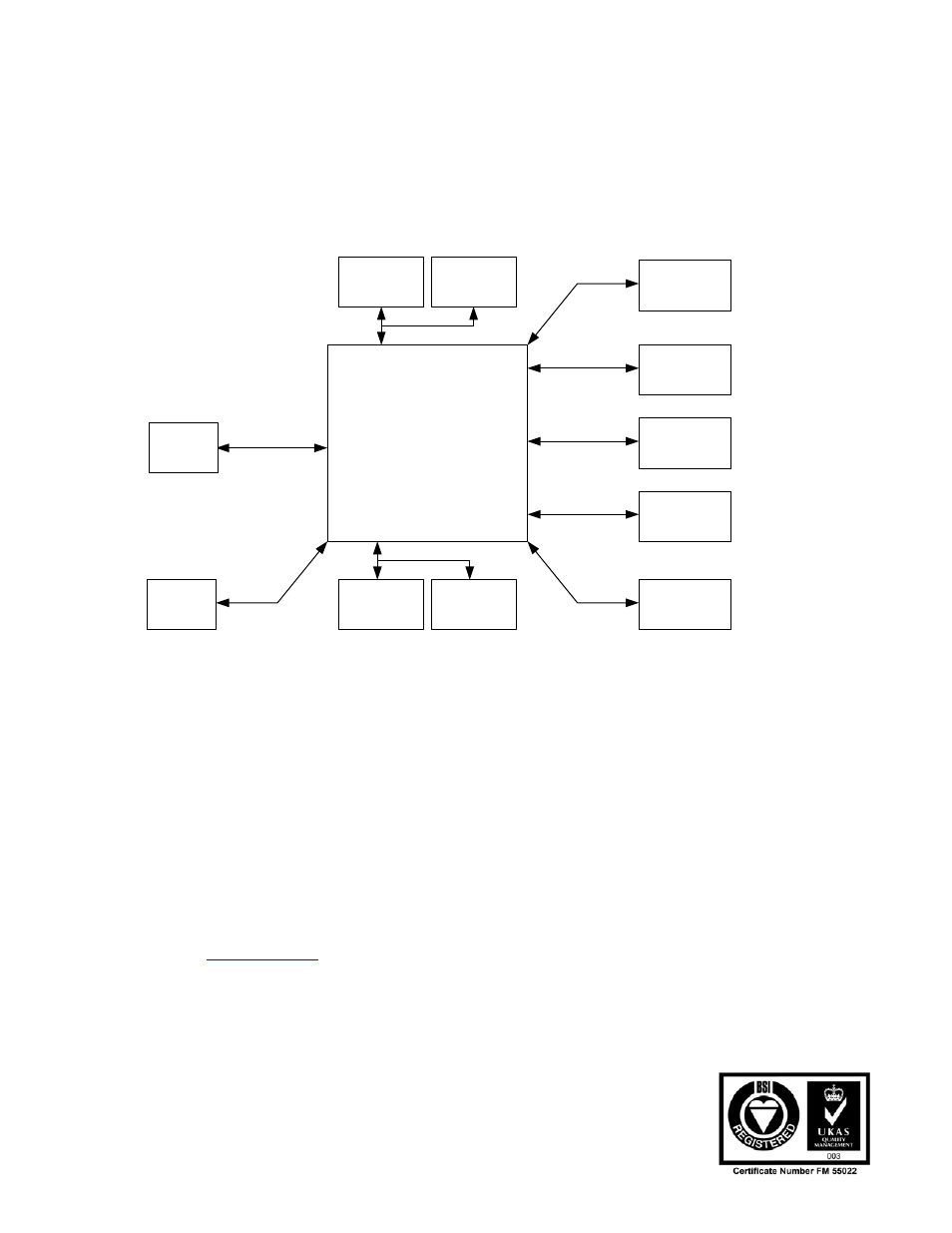
Architecture description
Bloc diagram
This section describes the major blocks of the SMT338-VP board.
Virtex-II Pro
XC2VP20-6 or 30-6
FF896 Package
508 / 556 IOs
256MBit
DDR SDRAM
256MBit
DDR SDRAM
512MBit for
Channel A
256MBit
DDR SDRAM
256MBit
DDR SDRAM
512MBit for
Channel B
4 RocketIO
Links for Channel A
(1GByte/s effective
Data throughput)
4 RocketIO
Links for Channel A
(1GByte/s effective
Data throughput)
SHB A
SHB B
Top and Bottom TIM
Connectors
Data, Clock and
Control (93)
Data, Clock and
Control (93)
DataTx (4d)
DataRx (4d)
DataTx (4d)
DataRx (4d)
ChA Data, Clock
and Control (60)
ChB Data, Clock
and Control (60)
ComPorts and
Control (59)
Debug IOs
and LEDs
Data (21)
Notes:
The numbers in brackets denote
the amount of FPGA IO pins
requires. 'd' is used for differential
pairs. 1d Will thus requre 2 IOs
SLB
FPGA
The SMT338-VP board uses a Xilinx Virtex II Pro (XC2VP20 or XC2VP30) to control
the data flow between the SMT338-VP board and external devices. The FPGA is
also used to implement the SHB, SLB, comport and DDR SDRAM interfaces.
The FPGA is configured via comport 3.
Memory
The SMT338-VP board contains four 166 MHz DDR SDRAM components (from
Micron:
MT46V16M16FN
) that provide each 32 MB of storage capacity.
The DDR SDRAM is a high-speed CMOS, dynamic random-access memory.
Examples of DDR SDRAM controller are provided by Xilinx.