Functional description – Sundance SMT338-VP User Manual
Page 14
Functional description
This section describes in detail the implementation of the board.
Memory banks
Memory is organised in two independent banks.
Both banks can be accessed at the same time.
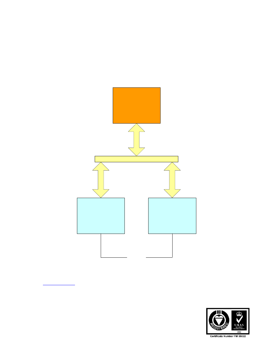
The following diagram shows how the DDR SDRAM components are organized
within a memory bank:
DDR SDRAM
32 Meg x 16 bits
1
6-bi
ts da
ta bus
DDR SDRAM
32 Meg x 16 bits
1
6-bi
ts da
ta bus
32-
b
its d
a
ta b
u
s
Chip Enable
FPGA
Figure 4: DDR SDRAM components bank organization
One bank is made from two 32M x 16-bits DDR SDRAM components
(
MT46V32M16FN
), each of them having a 16-bit data bus. Memory components are
accessed in pairs.
See also other documents in the category Sundance Equipment:
- SMT107 (16 pages)
- SMT6035 v.2.2 (39 pages)
- SMT6012 v.4.6 (22 pages)
- FC100 (12 pages)
- FC108 v.1.1 (10 pages)
- SMT6065 v.4.0 (45 pages)
- FFT v.2.1 (19 pages)
- SMT111 (18 pages)
- SMT118LT (10 pages)
- SMT118 (20 pages)
- SMT123-SHB (13 pages)
- SMT128 (15 pages)
- SMT145 (18 pages)
- SMT148 (35 pages)
- SMT130 v.1.0 (46 pages)
- SMT148FX (48 pages)
- SMT310Q (55 pages)
- PARS (70 pages)
- SMT166-FMC (52 pages)
- SMT166 (44 pages)
- SMT300Q v.1.6 (61 pages)
- SMT310 v.1.6 (50 pages)
- SMT317 (24 pages)
- SMT326v2 (24 pages)
- SMT338 (19 pages)
- SMT349 (32 pages)
- SMT339 v.1.3 (27 pages)
- SMT358 (25 pages)
- SMT351T (37 pages)
- SMT351 (25 pages)
- SMT350 (45 pages)
- SMT362 (30 pages)
- SMT365G (23 pages)
- SMT364 (37 pages)
- SMT373 (15 pages)
- SMT368 (24 pages)
- SMT370v3 (46 pages)
- SMT377 (22 pages)
- SMT381 2007 (31 pages)
- SMT381-VP (81 pages)
- SMT387 (42 pages)
- SMT391 (18 pages)
- SMT384 (47 pages)
- SMT390-VP (55 pages)