24 external fpga clock input, 25 fpga (virtex4 and spartan) configuration, External fpga clock input – Sundance SMT148FX User Manual
Page 24: Fpga (virtex4 and spartan) configuration
4.1.24 External FPGA Clock Input
Located near the DSP JTAG headers, connector J6 provides a direct connection to
the FPGA pin H17. This has 50 Ohm termination and is suitable for LVTTL
(maximum 3.3V) signals only.
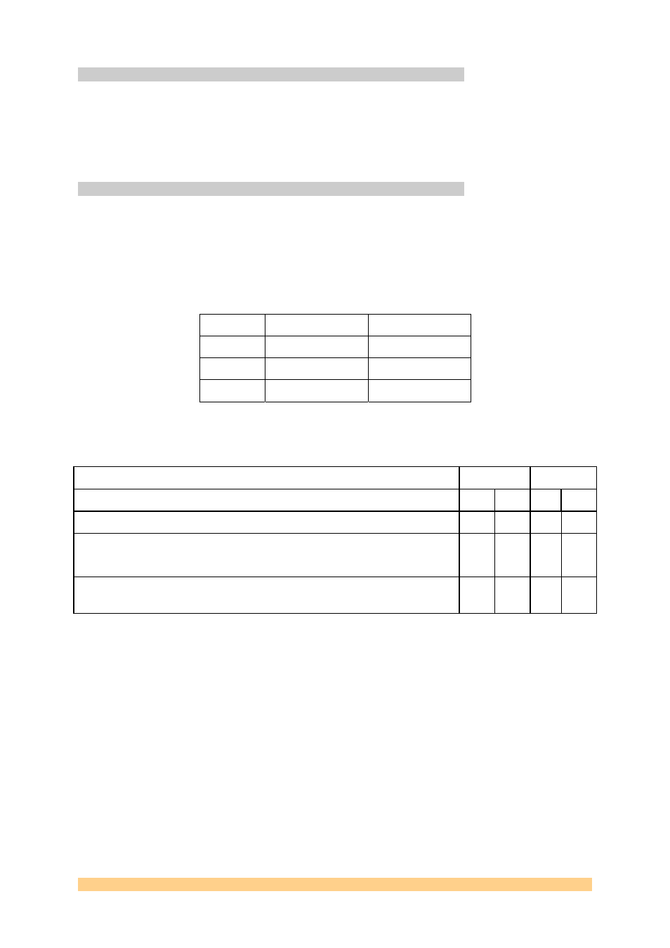
4.1.25 FPGA (Virtex4 and Spartan) configuration
The Virtex4 FPGA can be configured from flash, USB or ComPort. This is determined
by the setting of switch bank SW3, and is detailed in the following table. Note that
SW4-1 must be set to OFF.
The Jumpers [1-2] of SW3 control the Spartan configuration
The Jumpers [3-4] of SW3 control the Virtex4 configuration.
SW3
Position 2 or 4 Position 1 or 3
Flash
ON
ON
Comport
OFF
ON
USB ON OFF
Examples:
Virtex 4
Spartan
SW3 4
3
2
1
Both devices configure from Flash.
ON ON ON ON
Direct configuration via USB.
(needs a host application to send the bitstreams via USB)
ON OFF ON OFF
Configuration of Spartan via Flash and of Virtex 4 via CP3
connected to TIM site 1 CP0.
OFF ON ON ON
The Spartan is always the device configured first.
It is possible to download a new configuration to the FPGA using a Xilinx JTAG cable
connected to a PC and to JP6 on the SMT148FX carrier. This uses the standard 14-
way ribbon cable supplied by Xilinx. Refer to Xilinx document DS300 v3.1 page 8 for
details of the pinout.
User Manual SMT148FX
Page 24 of 48
Last Edited: 03/08/2009 11:42:00