Sundance SMT148FX User Manual
Page 11
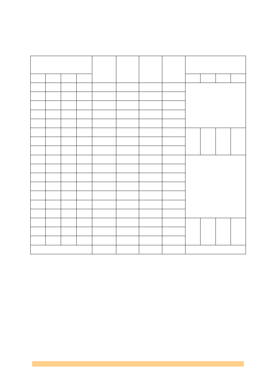
As the LVDS drivers are connected directly to the FX60 FPGA, they can be driven
from this device without need for the above McBSP method. The following table
shows the connectivity between the FPGA and the D-connectors (P2, 3, 4 & 5):
FPGA
signal pin
FPGA
enable pin
P2 P3 P4 P5
Signal D-
Conn
Pin
D-
Conn
Pin
Signal
P2 P3 P4 P5
GND 1 20 GND
D29
K29
M26
P31
RX0+ 2 21 RX0-
F31
C32
L30
P26
RX1+ 3 22 RX1-
E32
D32
L31
P27
RX2+ 4 23 RX2-
GND 5 24 GND
D31
E29
K31
M31
TX0+ 6 25 TX0-
E31 F29 K32 M32 TX1+
7
26
TX1- H27 J30 H32 N32
C29
J29
M25
P30
TX2+ 8 27 TX2-
GND 9 28 GND
GND 10
GND 11 29 GND
C30
L28
M28
P29
RX3- 12 30 RX3+
D30
L29
N27
R29
RX4- 13 31 RX4+
G31 H29 M30 R27 RX5-
14
32
RX5+
GND 15 33 GND
H28
J31
J32
P32
TX3- 16 34 TX3+
F30 J27 N28 R31 TX4-
17
35
TX4+ G32 H30 N30 R28
G30
K28
N29
R32
TX5- 18 36 TX5+
GND 19 37 GND
The LVDS transmitters are enabled in groups. Two groups per D-connector.
Eg. FPGA pin J30 is the transmitter enable for connector P3’s TX pins.
The LVDS receivers are continuously enabled and terminated by a 100 Ohm resistor.
User Manual SMT148FX
Page 11 of 48
Last Edited: 03/08/2009 11:42:00