Theory of operation, Open thermocouple detection, Isolated analog inputs – Measurement Computing CIO-DAS-TC User Manual
Page 13
CIO-DAS-TC User's Guide
Functional Details
13
Each thermocouple input is made through two screw terminals — one positive (+) and one negative (-).
Connect the thermocouple wires to the appropriate terminals, connect the CIO-STA-TC to the CIO-DAS-
TC, and your board is ready for use.
Note the polarity when connecting the thermocouples
Be careful to observe correct polarity when connecting thermocouple wires or extension wires.
Open thermocouple detection
The only user configurable option in the CIO-STA-TC is the open thermocouple detection resistors.
These are a series of 20 MΩ resistors that can be connected between the + terminal of the thermocouple,
and a known voltage that is larger than any allowable thermocouple output.
The 20 MΩ resistors are large enough so that they do not affect the readings from the thermocouples, but
if a thermocouple junction should open, a 20 MΩ drives the input voltage high enough so the software
can recognize that it is not a valid thermocouple reading.
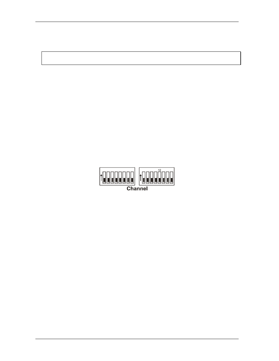
Open thermocouple detection circuitry is set via dip switches on the CIO-STA-TC. DIP switches are
labeled, and each channel has a switch. To enable open thermocouple detection for a channel, set the
switch to ON (up, towards the isothermal block). To disable the function, set the switch to OFF (down,
towards the outside of the board). The unit is shipped with open thermocouple detection disabled
The CIO-STA-TC is available by itself (MCC part number CIO-STA-TC), or as part of a kit that includes
the CIO-DAS-TC board and five foot shielded cable (MCC p/n CIO-DAS-TC.)
0 1 2 3
O
N
4 5 6 7
8 9 10 11
O
N
13 14 15
Theory of operation
Isolated analog inputs
The analog input section of the CIO-DAS-TC consists of a cold junction compensation (CJC) sensor
input, a 20 (differential) channel multiplexer, a precision 9.90 V source, an analog ground source, a
programmable gain amplifier suitable for scaling the seven thermocouple types, and a high frequency,
synchronous V-F A/D converter. During normal operation, the V-F converts the CJC input, calibrates the
gain at a Gain = 1 using the 9.9 V input, offset using the ground input, and measures the thermocouple or
voltage depending on the input type. The CJC and the gain/offset values are stored in an onboard RAM
for cold junction scaling and calibration. These parameters are sampled continuously. Refer to the block
diagram shown in Figure 4 on page 12.
The V-F converter is an Analog Devices AD652 SVFC (Synchronous V-F Converter) which offers full
scale frequency up to 2 MHz and extremely low linearity error. The 4 MHz clock for the V/F converter is
supplied by TIMER1 and passes through opto-isolation. The output of the V/F converter—passing back
through opto-isolation—is supplied to TIMER0. TIMER0 is gated on by TIMER2 for a period that
depends on the specified conversion frequency of 50 Hz, 60 Hz, or 400 Hz. At the end of the sampling
period, the count in TIMER0 represents the voltage input. In general, the longer the count time, the higher
the resolution and the better the noise reduction. However, in the case of periodic noise, the periodic
frequency (for example, 50, 60, and 400 Hz) is more effective in reducing the noise.