Measurement Computing DBK215 User Manual
Page 9
Pulse/Frequency Correlation to 68-pin SCSI
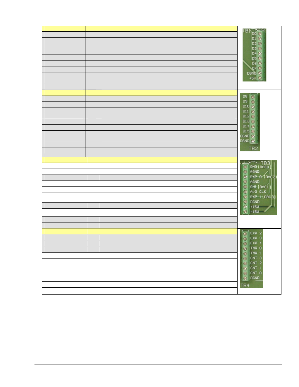
TB1
Pin Number and Description
D0
N/A
P3 Digital Port Bit 0
D1
N/A
P3 Digital Port Bit 1
D2
N/A
P3 Digital Port Bit 2
D3
N/A
P3 Digital Port Bit 3 TB1 is NOT USED
D4
N/A
P3 Digital Port Bit 4
D5
N/A
P3 Digital Port Bit 5
D6
N/A
P3 Digital Port Bit 6
D7
N/A
P3 Digital Port Bit 7
DGND
N/A
Digital Ground, Common
+5V
N/A
Expansion, +5 Volt Power
P3 – TB1 (not used)
TB2
Pin Number and Description
D8
N/A
P3 Digital Port Bit 8
D9
N/A
P3 Digital Port Bit 9
D10
N/A
P3 Digital Port Bit 10
D11
N/A
P3 Digital Port Bit 11 TB2 is NOT USED
D12
N/A
P3 Digital Port Bit 12
D13
N/A
P3 Digital Port Bit 13
D14
N/A
P3 Digital Port Bit 14
D15
N/A
P3 Digital Port Bit 15
DGND
N/A
Digital Ground, Common
DGND
N/A
Digital Ground, Common
P3 – TB2 (not used)
TB3
Pin Number and Description
CH0 (DAC0)
22
Analog Out; Analog DAC 0 Output
AGND
*
Analog Ground, Common; intended for use with DACs
EXP 0 (DAC2)
N/A
Analog Out; Analog DAC 2 Output
AGND
*
Analog Ground, Common; intended for use with DACs
CH1 (DAC1)
21
Analog Out; Analog DAC 1 Output
A/O CLK
1
Analog Out Clock; External DAC Pacer Clock Input/
Internal DAC Pacer Clock Output
EXP 1 (DAC3)
N/A
Analog Out; Analog DAC 3 Output
DGND
**
Digital Ground, Common
+15 V
N/A
Expansion, + 15 VDC
-15 V
N/A
Expansion, -15 VDC
P3 – TB3
TB4
Pin Number and Description
EXP 2
N/A
Reserved
EXP 3
N/A
Reserved
EXP 4
N/A
Reserved
TMR 0
3
P3 Timer 0 Output
TMR 1
37
P3, Timer 1 Output
CNT 3
38
P3 Counter 3 Input
CNT 2
4
P3 Counter 2 Input
CNT 1
39
P3 Counter 1 Input
CNT0
5
P3 Counter 0 Input
DGND
**
Digital Ground, Common
P3 – TB4
* The following SCSI Pins connect to Analog Common: 24, 27, 29, 32, 55, 56, 59, 64, and 67.
** The following SCSI Pins connect to Digital Common: 35, 36, 40, and 53.
DBK Option Cards and Modules
967894
DBK215 pg. 9