Measurement Computing DBK215 User Manual
Page 7
Analog I/O Correlation to 68-pin SCSI
Also see “Correlation to BNC Terminations (TB13 and TB14) on page DBK215-10.”
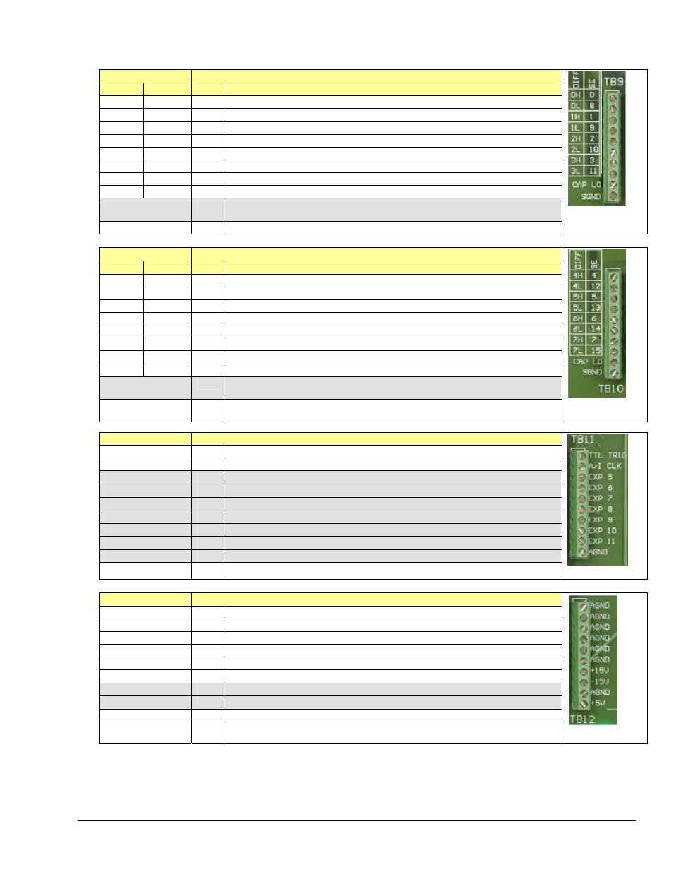
TB9
Pin Number and Description
DIFF
SE
0H
0
68
CH 0 IN (Single-Ended Mode) / CH 0 HI IN (Differential Mode)
0L
8
34
CH 8 IN (Single-Ended Mode) / CH 0 LO IN (Differential Mode)
1H
1
33
CH 1 IN (Single-Ended Mode) / CH 1 HI IN (Differential Mode)
1L
9
66
CH 9 IN (Single-Ended Mode) / CH 1 LO IN (Differential Mode)
2H
2
65
CH 2 IN (Single-Ended Mode) / CH 2 HI IN (Differential Mode)
2L
10
31
CH 10 IN (Single-Ended Mode) / CH 2 LO IN (Differential Mode)
3H
3
30
CH 3 IN (Single-Ended Mode) / CH 3 HI IN (Differential Mode)
3L
11
63
CH 11 IN (Single-Ended Mode) / CH 3 LO IN (Differential Mode)
FILT CAP LO
N/A
For RC filter networks install a wire jumper between the relevant FILT CAP LO and
AGND. Note that there is no association between FILT CAP LO and P4.
SGND
62
Signal Ground, Sense Common; reference ground, not for general use.
P1 – TB9
(Note 2)
TB10
Pin Number and Description
DIFF
SE
4H
4
28
CH 4 IN (Single-Ended Mode) / CH 4 HI IN (Differential Mode)
4L
12
61
CH 12 IN (Single-Ended Mode) / CH 4 LO IN (Differential Mode)
5H
5
60
CH 5 IN (Single-Ended Mode) / CH 5 HI IN (Differential Mode)
5L
13
26
CH 13 IN (Single-Ended Mode) / CH 5 LO IN (Differential Mode)
6H
6
25
CH 6 IN (Single-Ended Mode) / CH 6 HI IN (Differential Mode)
6L
14
58
CH 14 IN (Single-Ended Mode) / CH 6 LO IN (Differential Mode)
7H
7
57
CH 7 IN (Single-Ended Mode) / CH 7 HI IN (Differential Mode)
7L
15
23
CH 15 IN (Single-Ended Mode) / CH 7 LO IN (Differential Mode)
FILT CAP LO
N/A
For RC filter networks install a wire jumper between the
relevant FILT CAP LO and AGND.
SGND
62
Signal Ground, Sense Common; reference ground, not for general use.
P1 – TB10
(Note 2)
TB11
Pin Number and Description
TTL TRIG
6
TTL Trigger, Digital IN, External TTL Trigger Input
A/I CLK
2
A/I Clock, External ADC Pacer Clock Input/ Internal ADC Pacer Clock Output
EXP 5
N/A
Expansion 5. Digital OUT, external GAIN select bit 1
EXP 6
N/A
Expansion 6. Digital OUT, external GAIN select bit 0
EXP 7
N/A
Expansion 7. Digital OUT, external ADDRESS, select bit 3
EXP 8
N/A
Expansion 8. Digital OUT, external ADDRESS, select bit 2
EXP 9
N/A
Expansion 9. Digital OUT, external ADDRESS, select bit 1
EXP 10
N/A
Expansion 10. Digital OUT, external ADDRESS, select bit 0
EXP 11
N/A
Expansion 11. Simultaneous Sample and Hold (SSH)
AGND
*
Analog Ground, Common
P1 – TB11
TB12
Pin Number and Description
AGND
*
Analog Ground, Common
AGND
*
Analog Ground, Common
AGND
*
Analog Ground, Common
AGND
*
Analog Ground, Common
AGND
*
Analog Ground, Common
AGND
*
Analog Ground, Common
+ 15 V
N/A
Expansion, +15 V Power
- 15 V
N/A
Expansion, -15 V Power
AGND *
Common
Ground
+ 5 V
19
Expansion, +5 V Power
P1 – TB12
*The following SCSI Pins connect to Analog Common: 24, 27, 29, 32, 55, 56, 59, 64, and 67.
Note 2
: For TB9 and TB10, the filter network portion of the silkscreen is not shown. Instead, the DIFF and SE channel
identifiers have been moved next to the screws for ease in identification.
DBK Option Cards and Modules
967894
DBK215 pg. 7