Pcim-dda06/16 block diagram, Pcim-dda06/16 block diagram -2 – Measurement Computing PCIM-DDA06/16 User Manual
Page 8
PCIM-DDA06/16 User's Guide
Introducing the PCIM-DDA06/16
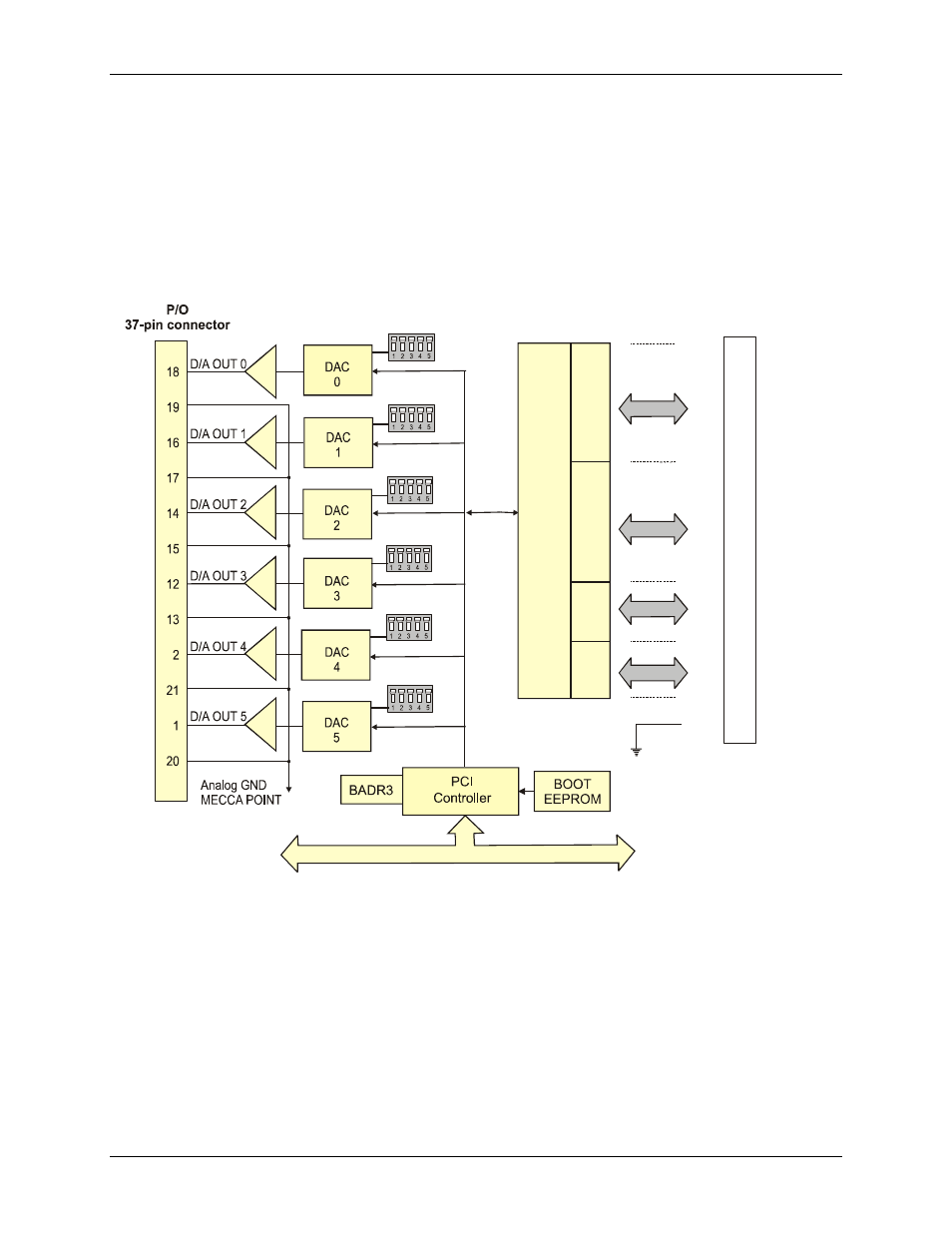
PCIM-DDA06/16 block diagram
The PCIM-DDA06/16 board consists of two functional sections: analog output and digital I/O. The digital I/O
section consists of a single 82C55, and a 24-line digital I/O chip. The analog output section consists of six
identical circuits, each consisting of a DAC, an OP27 output buffer, and a gain range control switch. You can
control each analog output individually, or control all six outputs simultaneously.
PCIM-DDA06/16 functions are illustrated in the block diagram shown here.
FIRSTPORTA Bit 0
Bit 1
Bit 2
Bit 3
Bit 4
Bit 5
Bit 6
Bit 7
FIRSTPORTB Bit 0
Bit 1
Bit 2
Bit 3
Bit 4
Bit 5
Bit 6
Bit 7
FIRSTPORTC Bit 0
Bit 1
Bit 2
Bit 3
FIRSTPORTC Bit 4
Bit 5
Bit 6
Bit 7
DGND
37
36
35
34
33
32
31
30
10
9
8
7
6
5
4
3
29
28
27
26
25
24
23
22
11
D
a
ta
P
a
th a
n
d C
o
nt
ro
l
FI
R
S
T
P
O
R
T
A
F
IR
S
TP
O
R
TB
C HI
8255
Digital I/O
Note: Digital I/O
pin assignments are
the same as for
the PCI-DIO24
P/O
37-pin conn.
PCI Bus - (5V, 32-bits, 33 MHz)
Gain switch
AD660
AD660
AD660
AD660
AD660
AD660
OP27
OP27
OP27
OP27
OP27
OP27
Gain switch
Gain switch
Gain switch
Gain switch
Gain switch
C L
O
1-2