2 simultaneous update jumper – Measurement Computing PC104-DAC06 User Manual
Page 7
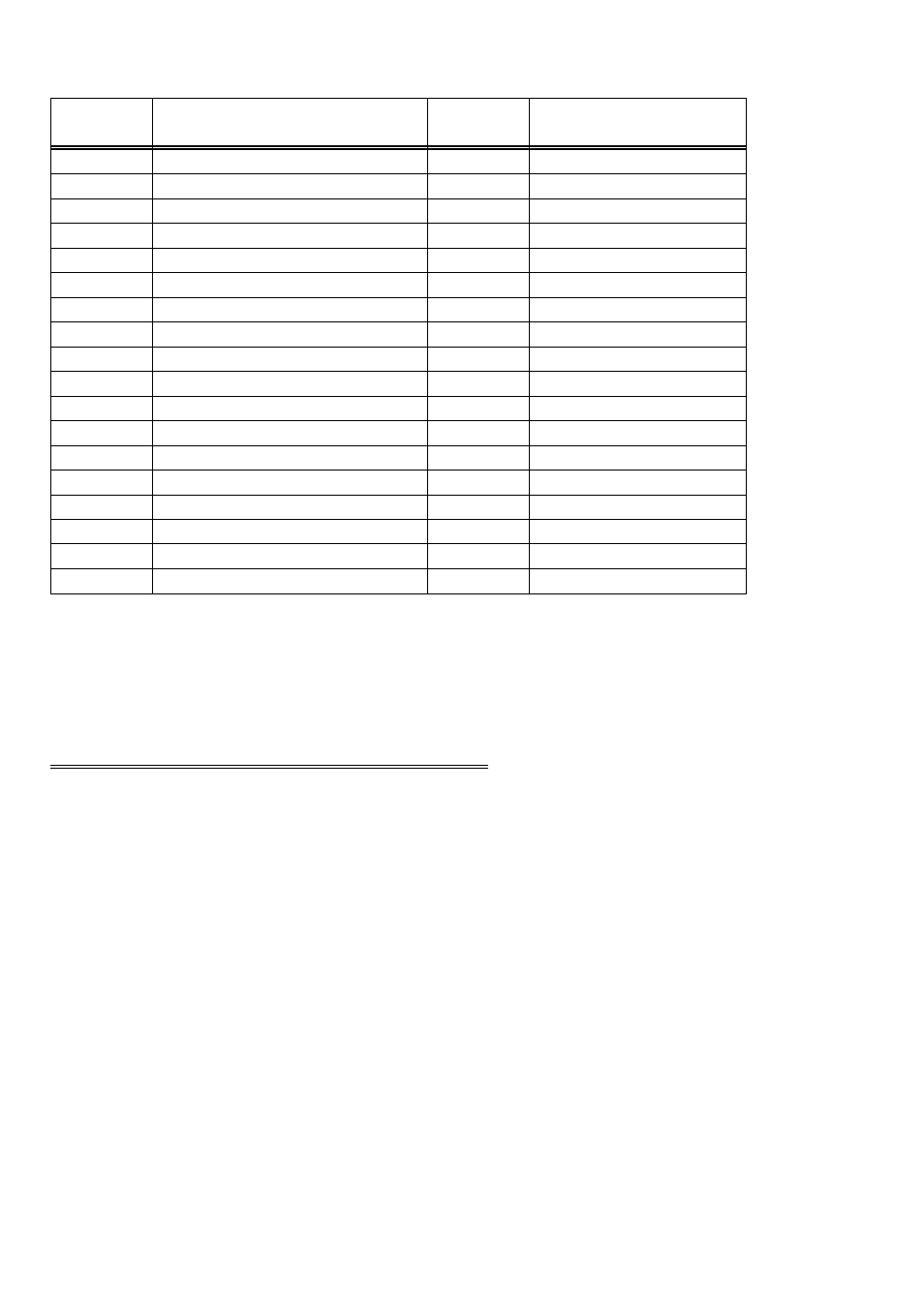
Table 3-1. PC I/O Addresses
SERIAL PORT
3F8-3FF
EGA
2B0-2BF
FLOPPY DISK
3F0-3F7
PARALLEL PRINTER
270-27F
SERIAL PORT
3E8-3EF
ALT BUS MOUSE
23C-23F
CGA
3D0-3DF
BUS MOUSE
238-23B
EGA
3C0-3CF
EXPANSION UNIT (XT)
210-21F
PARALLEL PRINTER
3BC-3BF
GAME CONTROL
200-20F
MDA
3B0-3BB
HARD DISK (AT)
1F0-1FF
SDLC
3A0-3AF
80287 NUMERIC CO-P (AT)
0F0-0FF
SDLC
380-38F
8237 #2 (AT)
0C0-0DF
PARALLEL PRINTER
378-37F
NMI MASK (XT)
0A0-0AF
HARD DISK (XT)
320-32F
8259 PIC #2 (AT)
0A0-0A1
PROTOTTYPE CARD
310-31F
DMA PAGE REGISTERS
080-08F
PROTOTYPE CARD
300-30F
CMOS RAM & NMI MASK (AT)
070-071
SERIAL PORT
2F8-2FF
8742 CONTROLLER (AT)
060-064
SERIAL PORT
2E8-2EF
8255 PPI (XT)
060-063
GPIB (AT)
2E0-2E7
8253 TIMER
040-043
EGA
2D0-2DF
8259 PIC #1
020-021
EGA
2C0-2CF
8237 DMA #1
000-00F
FUNCTION
HEX
RANGE
FUNCTION
HEX
RANGE
The PC104-DAC06 BASE switch may be set for address in the range of 000-3F0 so it
should not be hard to find a free address area for your PC104-DAC06. Once again, if
you are not using IBM prototype cards or some other board which occupies these
addresses, then 300-31Fh are free to use. Address not specifically listed, such as
390-39Fh, are free.
3.2 SIMULTANEOUS UPDATE JUMPER
The analog outputs can be jumpered so that new output data is held until two, four, or
six DACs have been loaded with new digital data. Then, as a group, those that are
jumpered for simultaneous outputs will have that new data sent to the voltage outputs.
Simultaneous update occurs whenever any addresses BASE + 0 through BASE + 11
are read.
The analog output chips are dual DACs. A single jumper sets both DACs on a single
chip to be either simultaneous TRANSFER or individual UPDATE.
3