Measurement Computing CIO-DAS08/JR/16 User Manual
Page 10
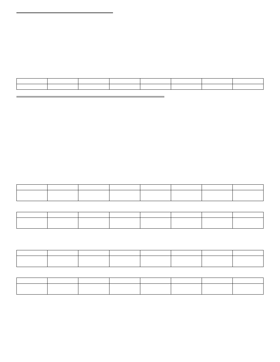
6.4 DIGITAL I/O CONTROL REGISTER
BASE ADDRESS + 3
This address contains two registers, one for outputs and one for inputs. The output register is latched and holds the last value written
to it. The input register is not latched. Each time the register is read, the current state of the inputs is passed through this port into the
computer.
WRITE = Set digital output port, all bits.
READ = Read digital input port, all bits, and update both D/As simultaneously with last values written to D/A output registers.
D0
D1
D2
D3
D4
D5
D6
D7
0
1
2
3
4
5
6
7
6.5 D/A CONTROL REGISTERS ( CIO-DAS08/JR/16-AO only)
Each D/A receives its data from a pair of 8-bit write-only registers. These registers contain the high byte and the low byte of the D/A
16-bit data word. The value written to these two registers determines the voltage output of the D/A chip. When in individual update
mode, the D/A outputs are updated when the high byte for the channel is written.
When in simultaneous mode, the D/A outputs are updated with the values in the D/A output registers when any register from BASE +0
to BASE + 7 is read.
The D/A output range can generally be calculated as [(#/65536) * 10V]
−
5V.
The #/65536 is a proportion of the Full Scale Range, which is +/-5V.
D/A 0 CONTROL REGISTERS
BASE ADDRESS + 4
DAC 0 LOW BYTE
DA0
LSB
DA1
DA2
DA3
DA4
DA5
DA6
DA7
0
1
2
3
4
5
6
7
BASE ADDRESS + 5
DAC 0 HIGH BYTE
DA8
DA9
DA10
DA11
DA12
DA13
DA14
DA15
MSB
0
1
2
3
4
5
6
7
D/A 1 CONTROL REGISTERS
BASE ADDRESS + 6
DAC 1 LOW BYTE
DA0
LSB
DA1
DA2
DA3
DA4
DA5
DA6
DA7
0
1
2
3
4
5
6
7
BASE ADDRESS + 7
DAC 1 HIGH BYTE
DA8
DA9
DA10
DA11
DA12
DA13
DA14
DA15
MSB
0
1
2
3
4
5
6
7
6