Fluke Biomedical 875 Victoreen User Manual
Page 29
Victoreen 875 High Range Containment Monitor
Operator Manual
4-8
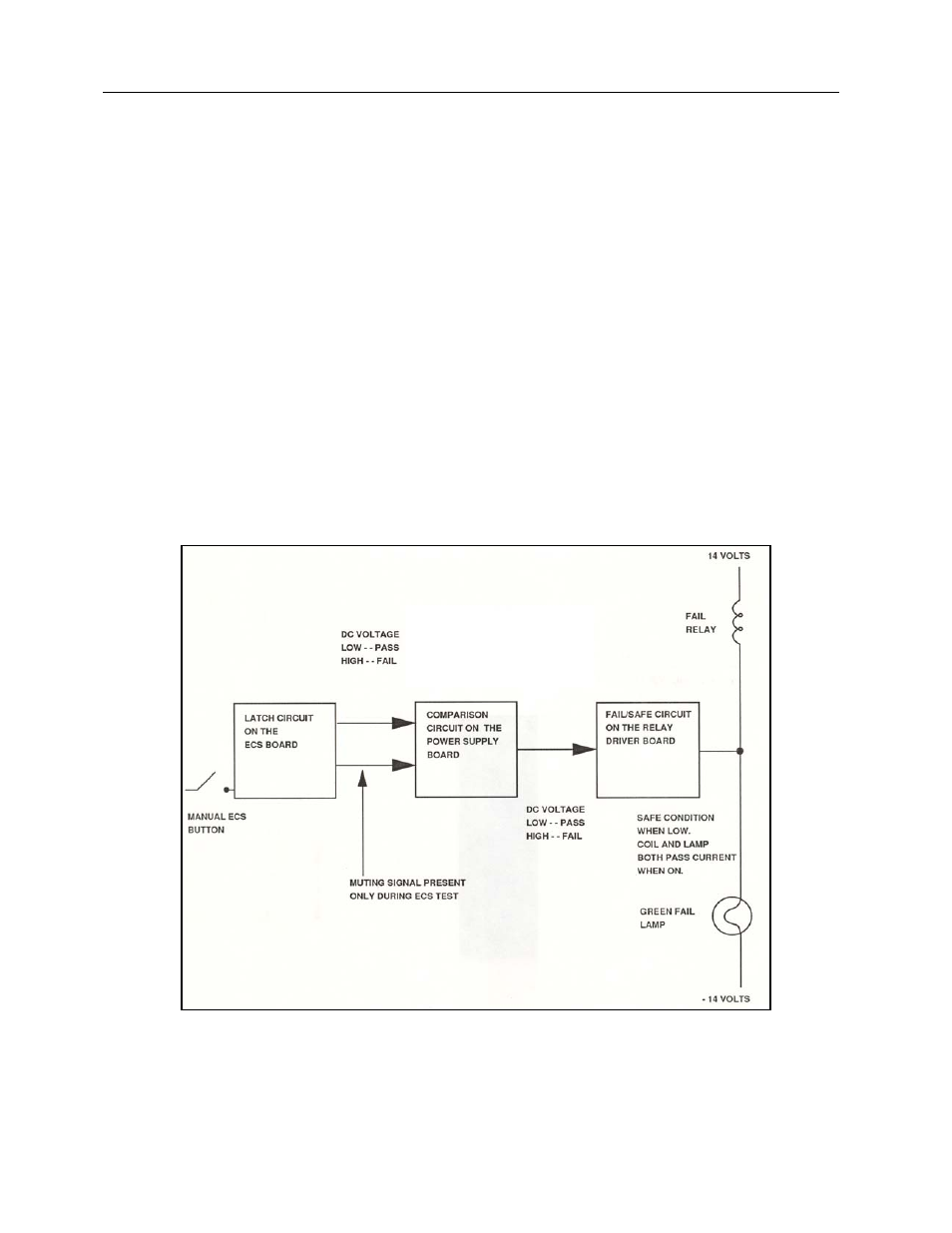
Monitoring Circuits of The ECS Board
rcuits of the ECS board is on terminal 1, the output on terminal 8. The input
erall circuit that monitors the ECS test also includes U2, described with the
p
Ultima
the charge integration adjustment potentiometer (CHARGE INTEG.
A
of
U20
ap
on
ch
This s
latch i
f
U202.
ss indication to a fail
ily
Figure 4-1. Block Diagram of ECS Test
The input to the monitoring ci
on terminal 1 is effectively proportional to the current produced in the detector by the application of the
high voltage ramp. The ov
ower supplies; and the SAFE/FAIL circuit on the relay driver printed circuit board.
tely, by the action of R218,
DJ.), charging capacitor C209, and other auxiliary elements, a DC voltage is produced on terminal 10
1, and an output voltage on pin 8 which results in an input to pin 10 of U208 which will be
proximately zero if the system is operative, and approximately + 15 V it a malfunction is present, or
annel power-up before the first automatic or manually initiated ECS test.
ignal is the input to the latch-and-flop circuit composed of the NOR circuits U202 (pins 1 to 13). The
s quiescent until triggered near the end of the ECS test period by the latch-enable input on pin 1 o
This trigger voltage will cause the output (pin 10 of U202) to flop from a pa
indication if a malfunction exists in the detector cable, or signal input circuit.
If the system is operative, a voltage that is low (6.2 V) will appear at terminal 8; if the system has a
malfunction, a voltage that is high (+15 V) will appear at this terminal (+15 V will appear momentar
immediately after power on). This voltage determines the action of a comparison circuit U4A, and the
output of U4A determines the action of the SAFE/FAIL circuit.
A block diagram of the entire monitoring circuit of the ECS test is shown in Figure 4-1.