Chapter 2 – DFI QB702-B User Manual
Page 16
www.dfi .com
Chapter 2 Hardware Installation
16
Chapter 2
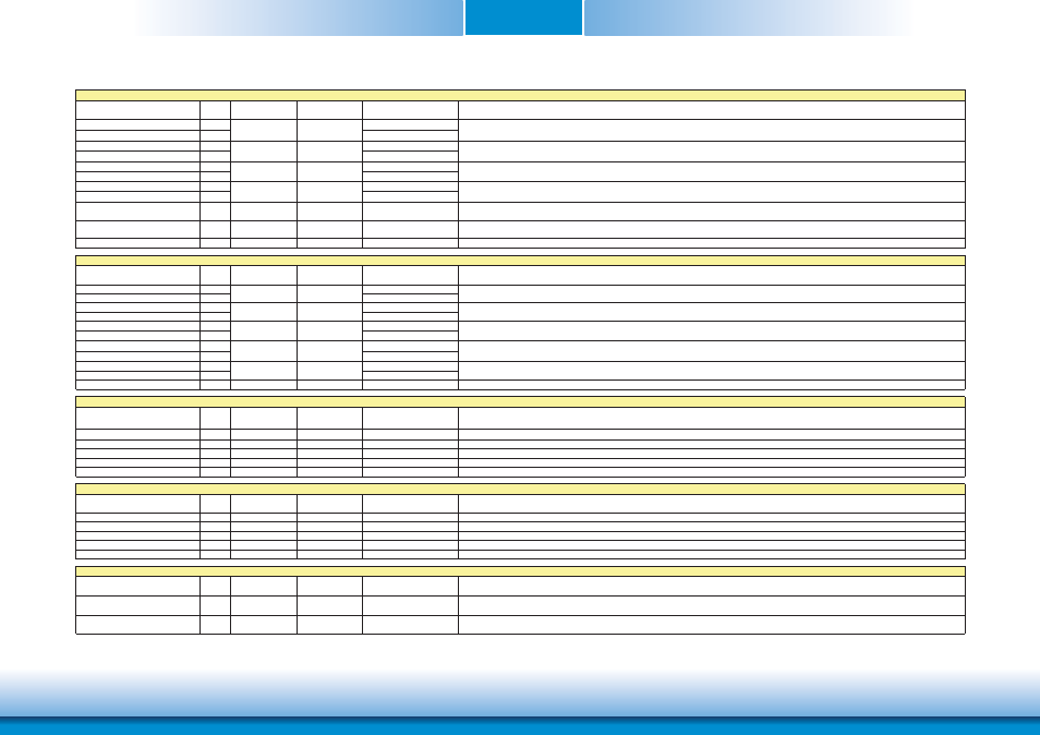
Signal
Pin#
Pin Type
Pwr Rail
/Tolerance
PU/PD (DFI-QB702)
Description
TMDS_CLK- (SDVO_BCLK-)
133
TMDS_CLK+ (SDVO_BCLK+)
131
TMDS_LANE0- (SDVO_BLUE-)
145
TMDS_LANE0+ (SDVO_BLUE+)
143
TMDS_LANE1- (SDVO_GREEN-)
139
TMDS_LANE1+ (SDVO_GREEN+)
137
TMDS_LANE2- (SDVO_RED-)
151
TMDS_LANE2+ (SDVO_RED+)
149
HDMI_CTRL_CLK (SDVO_CTRL_CLK)
152
I/O OD CMOS
3.3V/3.3V
DDC based control signal (clock) for HDMI device.
Note: Level shifters must be implemented on the carrier board for this signal in order to be compliant with the HDMI Specification.
HDMI_CTRL_DAT (SDVO_CTRL_DAT)
150
I/O OD CMOS
3.3V/3.3V
DDC based control signal (data) for HDMI device.
Note: Level shifters must be implemented on the carrier board for this signal in order to be compliant with the HDMI Specification
HDMI_HPD#
153
I CMOS
3.3V/3.3V
Hot plug detection signal that serves as an interrupt request.
Signal
Pin#
Pin Type
Pwr Rail
/Tolerance
PU/PD (DFI-QB702)
Description
DP_LANE3- (SDVO_BCLK-)
133
DP_LANE3+ (SDVO_BCLK+)
131
DP_LANE2- (SDVO_BLUE-)
145
DP_LANE2+ (SDVO_BLUE+)
143
DP_LANE1- (SDVO_GREEN-)
139
DP_LANE1+ (SDVO_GREEN+)
137
DP_LANE0- (SDVO_RED-)
151
DP_LANE0+ (SDVO_RED+)
149
DP_AUX- (SDVO_FLDSTALL-)
140
DP_AUX+ (SDVO_FLDSTALL+)
138
DP_HPD#
154
I CMOS
3.3V/3.3V
Hot plug detection signal that serves as an interrupt request.
Signal
Pin#
Pin Type
Pwr Rail
/Tolerance
PU/PD (DFI-QB702)
Description
LPC_AD[0..3]
185-188 I/O CMOS
3.3V/3.3V
Multiplexed Command, Address and Data.
LPC_FRAME#
190
O CMOS
3.3V/3.3V
LPC frame indicates the start of a new cycle or the termination of a broken cycle.
LPC_LDRQ#
192
I CMOS
3.3V/3.3V
LPC DMA request.
LPC_CLK
189
O CMOS
3.3V/3.3V
LPC clock.
SERIRQ
191
I/O CMOS
3.3V/3.3V
Serialized Interrupt.
Signal
Pin#
Pin Type
Pwr Rail
/Tolerance
PU/PD (DFI-QB702)
Description
SPI_MOSI
199
O CMOS
3.3V/3.3V
Master serial output/Slave serial input signal. SPI serial output data from Qseven module to the SPI device.
SPI_MISO
201
I CMOS
3.3V/3.3V
Master serial input/Slave serial output signal. SPI serial input data from the SPI device to Qseven module.
SPI_SCK
203
O CMOS
3.3V/3.3V
SPI clock output.
SPI_CS0#
200
O CMOS
3.3V/3.3V
SPI chip select 0 output.
SPI_CS1#
202
O CMOS
3.3V/3.3V
SPI Chip Select 1 signal is used as the second chip select when two devices are used. Do not use when only one SPI device is used.
Signal
Pin#
Pin Type
Pwr Rail
/Tolerance
PU/PD (DFI-QB702)
Description
CAN0_TX
129
O CMOS
3.3V/3.3V
CAN (Controller Area Network) TX output for CAN Bus channel 0.
In order to connect a CAN controller device to the Qseven module's CAN bus it is necessary to add transceiver hardware to the carrier board.
CAN0_RX
130
I CMOS
3.3V/3.3V
PU 10K to 3.3V
RX input for CAN Bus channel 0. In order to connect a CAN controller device to the Qseven module's CAN bus it is necessary to add transceiver hardware to the carrier
board.
I/O PCIE
Auxiliary channel used for link management and device control. Differential pair lines.
O PCIE
DisplayPort differential pair lines lane 1.
O PCIE
DisplayPort differential pair lines lane 0.
O PCIE
DisplayPort differential pair lines lane 3.
O PCIE
DisplayPort differential pair lines lane 2.
DisplayPort Interface Signals
HDMI Interface Signals
O TMDS
O TMDS
O TMDS
O TMDS
TMDS differential pair clock lines.
TMDS differential pair lines lane 0.
TMDS differential pair lines lane 1.
TMDS differential pair lines lane 2.
LPC Interface Signals
SPI Interface Signals
CAN Bus Interface Signals
TMDS
TMDS
TMDS
TMDS
DP
DP
DP
DP
DP