Mxm connector signal description, Chapter 2 mxm connector signal description – DFI QB702-B User Manual
Page 13
www.dfi .com
Chapter 2 Hardware Installation
13
Chapter 2
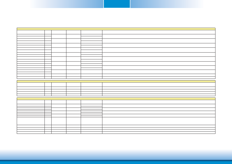
MXM Connector Signal Description
Signal
Pin#
Pin Type
Pwr Rail
/Tolerance
PU/PD (DFI-QB702)
Description
PCIE0_RX+
180
PCIE0_RX-
182
PCIE0_TX+
179
PCIE0_TX-
181
PCIE1_RX+
174
PCIE1_RX-
176
PCIE1_TX+
173
PCIE1_TX-
175
PCIE2_RX+
168
PCIE2_RX-
170
PCIE2_TX+
167
PCIE2_TX-
169
PCIE3_RX+
162
PCIE3_RX-
164
PCIE3_TX+
161
PCIE3_TX-
163
PCIE_CLK_REF+
155
PCIE_CLK_REF-
157
PCIE_WAKE#
156
I CMOS
3.3V Suspend/3.3V
PU 10K to 3.3V Suspend
PCI Express Wake Event: Sideband wake signal asserted by components requesting wakeup.
PCIE_RST#
158
O CMOS
3.3V/3.3V
Reset Signal for external devices.
Signal
Pin#
Pin Type
Pwr Rail
/Tolerance
PU/PD (DFI-QB702)
Description
EXCD0_CPPE#
177
I CMOS
3.3V
PU 10K to 3.3V
ExpressCard slot #0 capable card request
EXCD0_PERST#
171
O CMOS
3.3V
PU 10K to 3.3V
ExpressCard slot #0 reset.
EXCD1_CPPE#
178
I CMOS
3.3V
PU 10K to 3.3V
ExpressCard slot #1 capable card request.
EXCD1_PERST#
172
O CMOS
3.3V
ExpressCard slot #1 reset.
Signal
Pin#
Pin Type
Pwr Rail
/Tolerance
PU/PD (DFI-QB702)
Description
GBE_MDI0+
12
GBE_MDI0-
10
GBE_MDI1+
11
GBE_MDI1-
9
GBE_MDI2+
6
GBE_MDI2-
4
GBE_MDI3+
5
GBE_MDI3-
3
GBE_CTREF
15
I/O GB_LAN
GB_LAN
Reference voltage for carrier board Ethernet channel 0 magnetics center tap.
The reference voltage is determined by the requirements of the module's PHY and may be as low as 0V and as high as 3.3V.
The reference voltage output should be current limited on the module. In a case in which the reference is shorted to ground, the current must be limited to 250mA
or less.
GBE_LINK#
13
O CMOS 3.3V PP
3.3V/3.3V
PU 10K to 2.5V
Ethernet controller 0 link indicator, active low.
GBE_LINK100#
7
O CMOS 3.3V PP
3.3V/3.3V
Ethernet controller 0 100Mbit/sec link indicator, active low.
GBE_LINK1000#
8
O CMOS 3.3V PP
3.3V/3.3V
Ethernet controller 0 1000Mbit/sec link indicator, active low.
GBE_ACT#
14
O CMOS 3.3V PP
3.3V/3.3V
PU 10K to 2.5V
Ethernet controller 0 activity indicator, active low.
I/O GB_LAN
Media Dependent Interface (MDI) differential pair 3. The MDI can operate in 1000, 100, and 10Mbit/sec modes.This signal pair is used for all modes.
PCI Express Interface Signals Descriptions
I PCIE
I PCIE
I PCIE
O PCUE
O PCUE
O PCUE
PCI Express channel 0, Receive Input differential pair.
PCI Express channel 0, Transmit Output differential pair.
PCI Express channel 1, Receive Input differential pair.
PCI Express channel 1, Transmit Output differential pair.
PCI Express channel 2, Receive Input differential pair.
PCI Express channel 2, Transmit Output differential pair.
PCI Express channel 3, Receive Input differential pair.
PCI Express channel 3, Transmit Output differential pair.
I PCIE
O PCUE
PCIE
PCIE
PCIE
PCIE
PCIE
PCIE
O PCUE
PCIE
PCI Express Reference Clock for Lanes 0 to 3.
Express Card Support Pins
Gigabit Ethernet Signals
I/O GB_LAN
Media Dependent Interface (MDI) differential pair 0. The MDI can operate in 1000, 100, and 10Mbit/sec modes.This signal pair is used for all modes.
I/O GB_LAN
Media Dependent Interface (MDI) differential pair 1. The MDI can operate in 1000, 100, and 10Mbit/sec modes.This signal pair is used for all modes.
PCIE
PCIE
GB_LAN
GB_LAN
GB_LAN
GB_LAN
I/O GB_LAN
Media Dependent Interface (MDI) differential pair 2. The MDI can operate in 1000, 100, and 10Mbit/sec modes.This signal pair is used for all modes.