Chapter 3 – DFI OT905-B series User Manual
Page 22
www.dfi .com
Chapter 3 Hardware Installation
22
Chapter 3
Signal
Pin#
Pin Type
Pwr Rail /Tolerance
PU/PD
Description
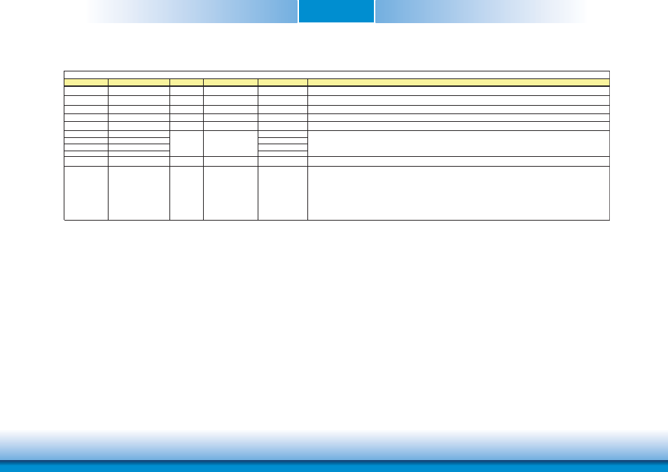
PCI Signals Descriptions
PCI_RESET#
C23
O CMOS
3.3V Suspend/ 5V
PCI Reset output, active low.
PCI_LOCK#
C35
I/O CMOS
3.3V / 5V
PU 8.2K to 3.3V
PCI Lock control line, active low.
PCI_SERR#
D33
I/O OD CMOS 3.3V / 5V
PU 8.2K to 3.3V
System Error: SERR# may be pulsed active by any PCI device that detects a system error condition.
PCI_PME#
C15
I CMOS
3.3V Suspend/ 5V
PU 10K to 3.3VSB
PCI Power Management Event: PCI peripherals drive PME# to wake system from low-power states S1–S5.
PCI_CLKRUN#
D48
I/O CMOS
3.3V / 5V
PU 8.2K to 3.3V
Bidirectional pin used to support PCI clock run protocol for mobile systems.
PCI_IRQA#
C49
PU 8.2K to 3.3V
PCI_IRQB#
C50
PU 8.2K to 3.3V
PCI_IRQC#
D46
PU 8.2K to 3.3V
PCI_IRQD#
D47
PU 8.2K to 3.3V
PCI_CLK
D50
O CMOS
3.3V / 3.3V
PCI 33MHz clock output.
PCI_M66EN
D49
I CMOS
3.3V / 5V
Module input signal indicates whether an off-Module PCI device is
capable of 66MHz operation. Pulled to GND by Carrier Board device or
by Slot Card if the devices are NOT capable of 66 MHz operation.
If the Module is not capable of supporting 66 MHz PCI operation, this
input may be a no-connect on the Module.
If the Module is capable of supporting 66 MHz PCI operation, and if this
input is held low by the Carrier Board, the Module PCI interface shall
operate at 33 MHz.
I CMOS
3.3V / 5V
PCI interrupt request lines.