Elenco Pocket Dice User Manual
Page 5
repeat the process with two showing on the die.
The output of IC2 also drives IC3. This results in
IC3 output changing in step with IC2, but at a slower
rate.
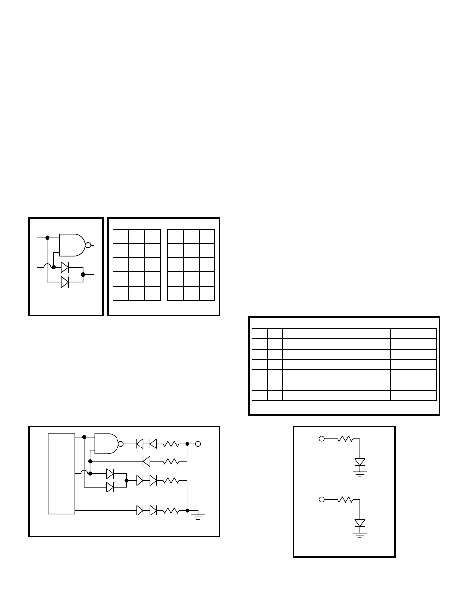
THE DECODER CIRCUIT
The decoder circuit takes the output of the
presettable counter and lights the correct LEDs.
Figure 4 shows the decoder circuit. It consists of a
NAND gate and an OR gate. The OR gate is
formed by two diodes. The purpose of the decoder
circuits is to “decode” the outputs of pins 4, 5 and 6
of IC2 or IC3 to light the correct LEDs. The truth
tables for the NAND and the OR gates are shown in
Figure 5. They show the output C versus the inputs
A and B. Thus, if the inputs of the NAND gate are
both low (0), the output will be high (1).
Figure 6 shows the wiring of the LEDs to the NAND
and OR gates output. Note that when IC pin 10 is
low, LED D2 and D1 will light. Also, when pin 5 or 6
of IC2 are high, LEDs D4 and D5 will light. Figure 7
shows which LEDs are being lit as a result of the
outputs of pin 4, 5 and 6 of IC2 or IC3.
Let’s go through a couple of decodings to see how
it works. Refer to Figures 6 and 7. Remember an
LED will light when the cathode is low and the
anode is high as shown in Figure 8.
When the die displays a one, only LED D3 will light.
For this to happen, output pin 4, 5 and 6 or IC2 will
have to go low (0) and the following will result.
1) D3 turns on as its cathode will be low.
2) The input of the NAND gate is low therefore its
output will be high. D2 and D1 will not light.
3) The input of the OR gate is low, so its output
will be low. Thus, D4 and D5 will not light.
4) Pin 4 of IC2 is low, therefore LED D6 and D7
will not light.
Let’s try another number - 3. Here we must light
LEDs D3, D4 and D5. The output of pin 4 is low, pin
5 and pin 6 low (0, 1, 0).
1) Pin 6 is low, therefore LED D3 will light.
2) Pin 5 is high, Therefore the outputs of the OR
gate will be high, lighting LED D4 and D5.
3) Pin 4 is low, therefore LEDs D6 and D7 will not
light.
4) The inputs of the NAND gate are high and low,
therefore the NAND gate output will be high
and LEDs D1 and D2 will not light.
Try to figure out the other four patterns. It actually
can be fun.
-4-
Figure 4
Figure 5
Figure 7
Figure 8
A B C
0 0 1
1 0 1
0 1 1
1 1 0
A B C
0 0 0
1 0 1
0 1 1
1 1 1
NAND
OR
4
5
6
LEDs Lit
Die Number
1
1
1
D4, D1, D7, D6, D2, D5
Six
1
1
0
D4, D7, D6, D5, D3
Five
1
0
1
D4, D7, D6, D5
Four
0
1
0
D4, D3, D5
Three
0
0
1
D4, D5
Two
0
0
0
D3
One
Pins on IC2
NAND Gate
OR Gate
Figure 6
IC2
9
8
5
6
4
D7 D6
D5 D4
D2 D1
D3
10
D16
D15
+
Current
Limiting
Resistors
Input High
Input Low
0V
9V
Lit
Not Lit