Pclta-20 board layout, P1 and p2 pci bus connector, Mechanical considerations – Echelon PCLTA Network Interface User Manual
Page 20: Pcc-10 board layout, Network port

12
Electrical and Mechanical Interfaces
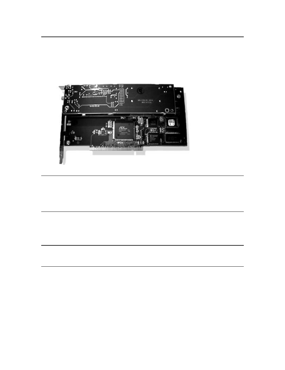
PCLTA-20 Board Layout
The following figure shows the layout of the PCLTA-20/SMX Interface. This card has a header
connector for an SMX transceiver and does not have an integral transceiver. Attach the SMX
transceiver in accordance with the manufacturer’s instructions – see the L
ON
W
ORKS
®
SMX™
Transceiver Installation Instructions document 078-0145-01 version D or later if using an Echelon
SMX transceiver.
P1 and P2 PCI Bus Connector
The pinout of the P1 and P2 connector terminals is the standard pinout for the 32-bit PCI bus used in
Windows-compatible computers. The power drawn from the host is 250 mA @ 5 VDC, typical. Actual
power consumed for the SMX or protocol analyzer card will vary according to the power needs of the
selected SMX transceiver.
Mechanical Considerations
The PCLTA-20/SMX card measures 3.69” (9.4 cm) H x 7.36” (18.7 cm) L. It is equipped with a full-
height chassis bracket. If a PLM SMX transceiver is used, two PCI slots must be dedicated to the card
due to the wider-width of the assembled PCLTA-20/PLM card.
PCC-10 Board Layout
The following section describes the PCC-10 board.
Network Port
The PCC-10 has a 15-pin network port connector for interfacing with a free topology or link power
channel, and for connecting external transceiver pods.
The following figure shows the numbering scheme of the 15-pin Hirose male connector on the PCC-10
card (the top of the PCC-10 card is the side with the product label).
