1 overview, Block diagram, 1overview – ADLINK LEC-BTS User Manual
Page 5: Pin smarc connector, 1 block diagram, Intel® e3800 series soc (system on chip)

Overview
1
LEC-BTS
1
Overview
This initial manual version presents a general overview of the LEC-BTS. After reviewing this
document you should understand the following features of the LEC-BTS.
Functional Block Diagram
Major Component (IC) Locations and Descriptions
Connector, Switch, and LED Locations and Descriptions
Specifications
SMARC Interface Signal Definitions and Debug Interface Signal Definitions
NOTE: Refer to
http://www.sget.org/standards/smarc.html
for SMARC specifications. Please
refer to BSP readme documents in the Quick Drive for BSP installation instructions.
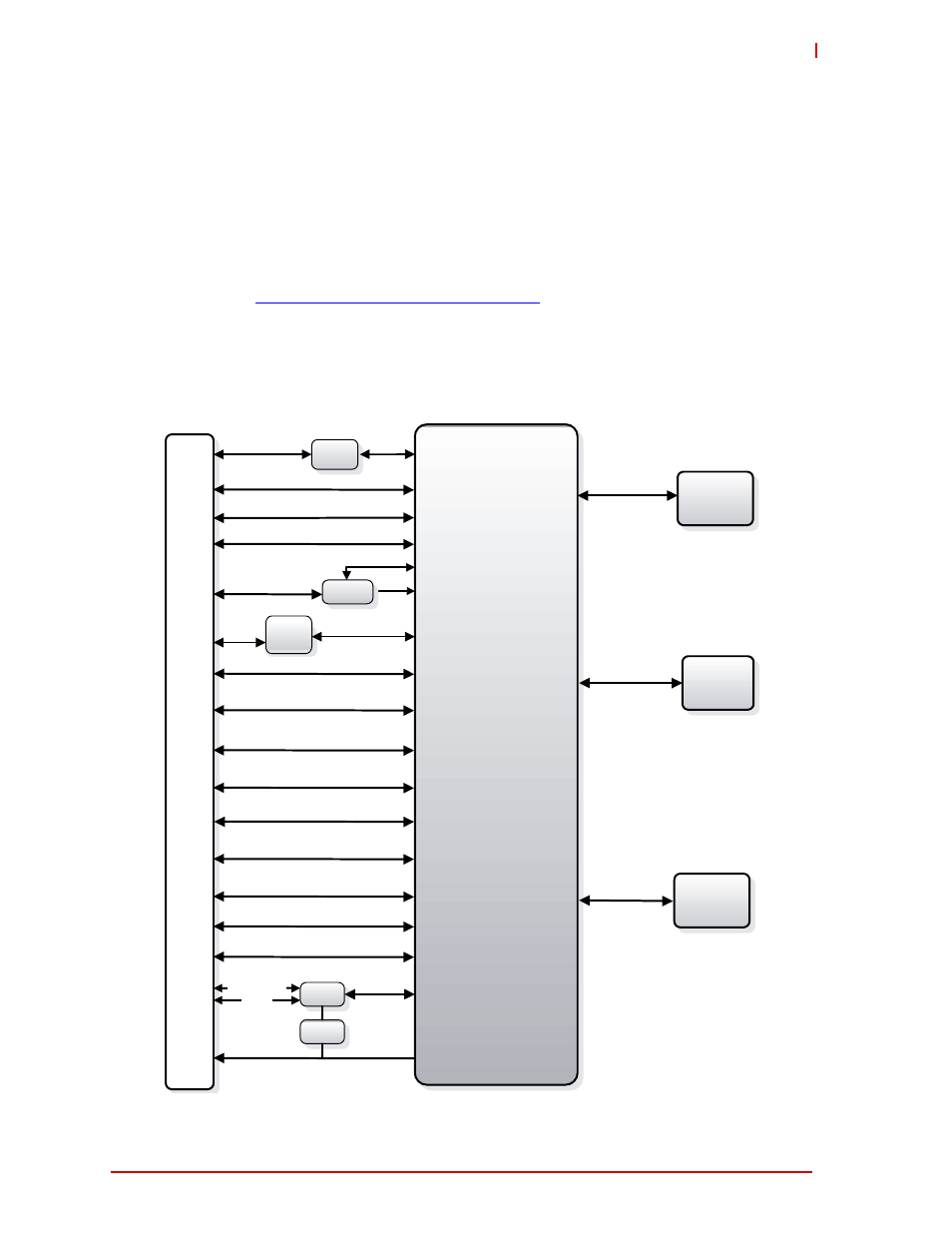
1.1 Block Diagram
Figure 1-1 represents the component functions of the module.
Figure 1-1: Functional Block Diagram
314-pin SMARC Connector
Intel®
E3800 Series
SoC
(System on Chip)
LVDS 18/24-bit
Single Channel
LVDS
Converter
RTD2136
DDI0
LPC
SPI
2x I2C
(GP/LVDS)
2x I2C (PM/CAM)
BOOT Select
Power Management
SDIO
DDI1 (HDMI)
LAN
Controller
i210IT
SATA0
Camera Support (CSI 4L/1L)
Audio (HDA and I2S)
USB 3.0 on AFB
USB 2.0, ports 0,1,2
PCIe x1, PCIe ports 1,2,3
PCIe x1
2x Serial (including RTS/CTS) +
PCU-UART (only RX/TX)
12x GPIO
(Five reserved for CSI)
SMB
MMC
GPIO
Expander
SMBus
INT
Gb
Ethernet
BMC
HWM
SPI
BIOS
Debug
DB40
Connector
DDR3L
1066/1333MHz
DDR3L
On-Board
2/4 GB
Memory
Power
Management
IC
IDTP9145
LEC_BTS_blk_diag_b
