2 block diagram, 1 adlink gpib interface cards block diagram, Block diagram – ADLINK USB-3488A User Manual
Page 38: Adlink gpib interface cards block diagram

30
Operation
Theory
3.2
Block Diagram
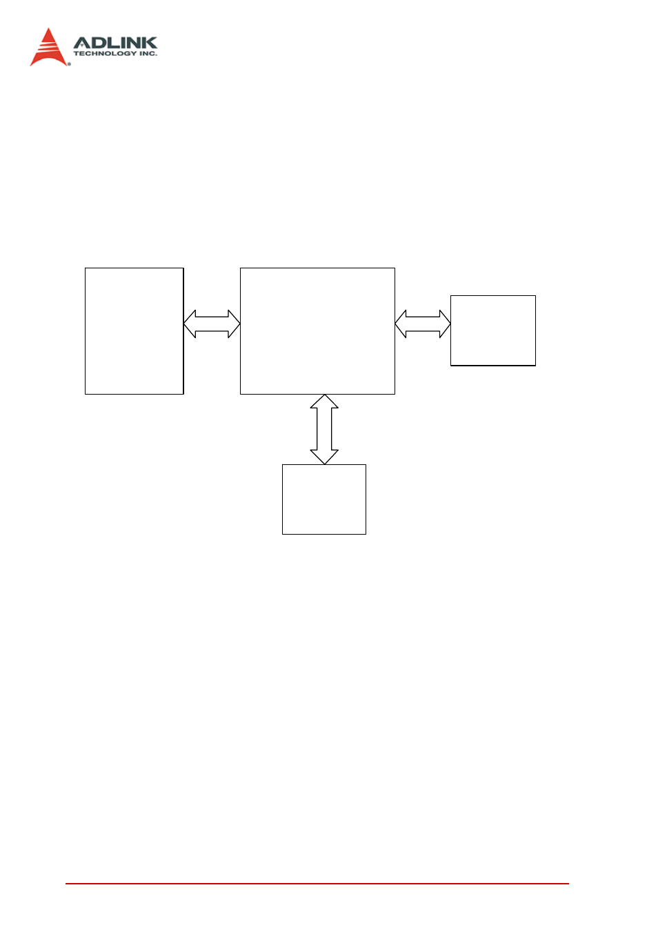
3.2.1 ADLINK GPIB Interface Cards Block Diagram
ADLINK’s LPCI-3488A and PXI-3488 GPIB interface cards include
a 2 KB FIFO inside the FPGA IP to maximize data transfer rates.
Its state-of-the-art state machine in the CPLD coordinates the data
flow between the PCI controller, FIFO and GPIB bus.
Figure 3-2: Block Diagram of ADLINK GPIB Interface Cards
The FIFO can buffer data from the master (either from the PCI
controller or external device) when the target is busy. Efficiency is
thus significantly improved when transferring large blocks of data.
FPGA
GPIB IP
(Built-in 2 KB FIFO)
PCI
Controller
Bus
Transceiver/
Receiver
CPLD
See also other documents in the category ADLINK Hardware:
- USB-1901 (84 pages)
- USB-1210 (54 pages)
- USB-2401 (60 pages)
- USB-7230 (50 pages)
- USB-2405 (56 pages)
- DAQe-2010 (92 pages)
- DAQe-2204 (100 pages)
- DAQe-2213 (94 pages)
- DAQe-2501 (74 pages)
- PXI-2010 (84 pages)
- PXI-2020 (60 pages)
- PXI-2501 (62 pages)
- cPCI-9116 (98 pages)
- ACL-8112 Series (92 pages)
- ACL-8112 Series (93 pages)
- ACL-8112 Series (94 pages)
- ACL-8216 (75 pages)
- ACL-8111 (61 pages)
- PCM-9112+ (10 pages)
- PCM-9112+ (94 pages)
- cPCI-6216V (47 pages)
- ACL-6126 (28 pages)
- ACL-6128A (40 pages)
- PCM-6308V+ (52 pages)
- PCM-6308V+ (4 pages)
- PCI-7444 (82 pages)
- PCI-7434 (48 pages)
- PCI-7234 (56 pages)
- PCI-7260 (66 pages)
- PCI-7258 (38 pages)
- PCI-7256 (48 pages)
- PCI-7250 (48 pages)
- LPCI-7250 (48 pages)
- PCI-7396 (65 pages)
- PCI-7296 (59 pages)
- PCI-8554 (67 pages)
- PCIe-7360 (94 pages)
- PCIe-7350 (86 pages)
- PCIe-7300A (114 pages)
- PCIe-7200 (51 pages)
- PCI-7300A (112 pages)
- PCI-7300A (83 pages)
- PCI-7200 (96 pages)
- cPCI-7300 (82 pages)
- cPCI-7300 (83 pages)
