Filter, 4 dma data transfer, Dma data transfer – ADLINK PCIe-9529 User Manual
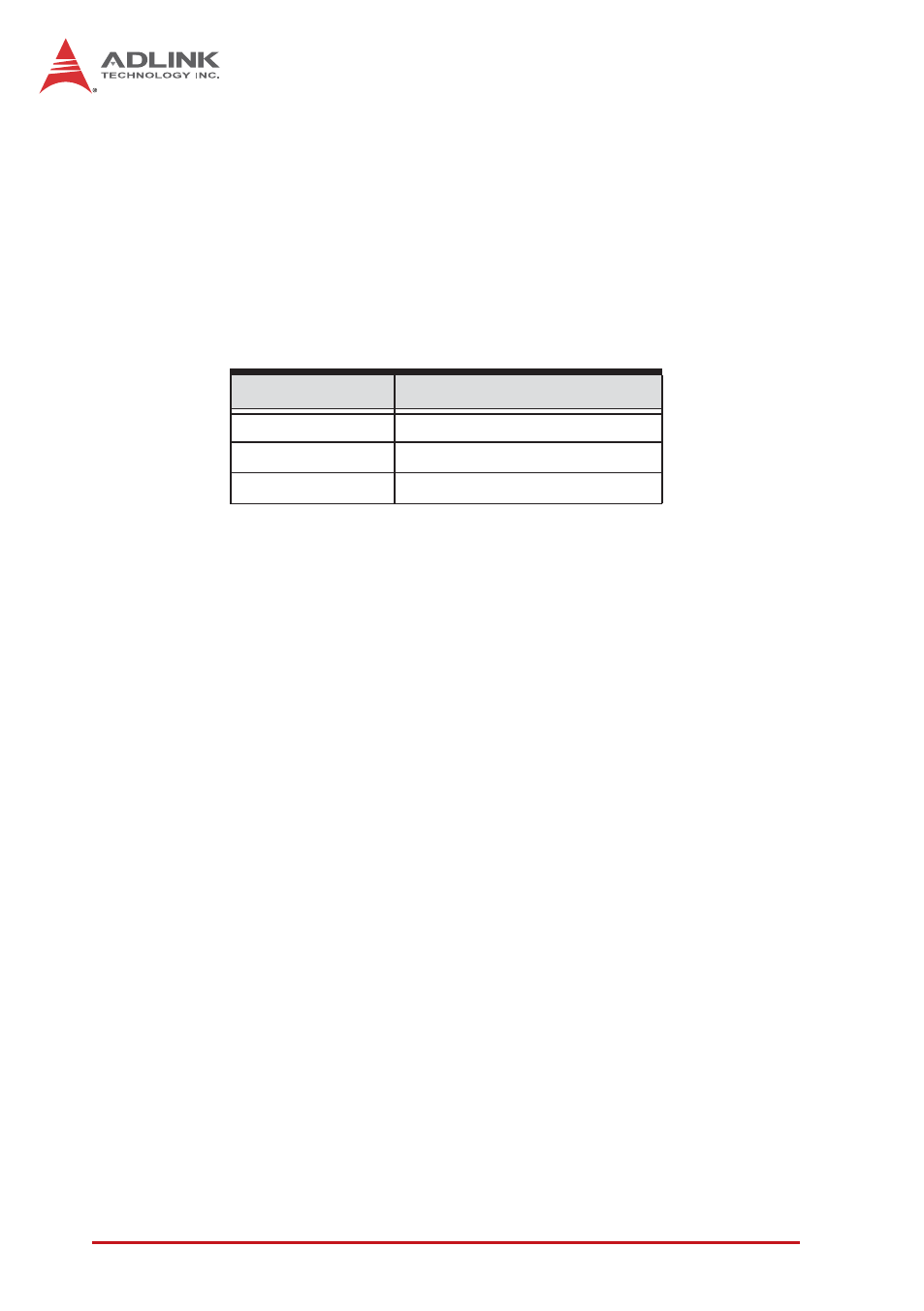
Page 30: Table 3-3: adc sample rates vs dds output clock

20
Operations
at 27.648MS/s, 256 times the sampling rate. The 1-bit 27.648MS/s
data streams from 1-bit ADC to its internal digital filter circuit to
produce 24-bit data at 108kS/s. The noise shaping removes quan-
tization noise from low frequency to high frequency. At the last
stage, the digital filter improves ADC resolution and removes high
frequency quantization noise. The relationship between ADC sam-
ple rate and DDS output clock is as follows.
Table 3-3: ADC Sample Rates vs DDS Output Clock
Filter
Each channel has a two-pole lowpass filter. The filters limit band-
width of the signal path and reject wideband noise.
3.2.4
DMA Data Transfer
The PCIe-9529, as a PCIe Gen1 X 4 device, provides a 192KS/s
sampling rate ADC, generating a 3.072 MByte/second rate. To
provide efficient data transfer, a PCI bus-mastering DMA is essen-
tial for continuous data streaming, as it helps to achieve the full
potential PCI Express bus bandwidth. The bus-mastering control-
ler releases the burden on the host CPU since data is directly
transferred to the host memory without intervention. Once analog
input operation begins, the DMA returns control of the program.
During DMA transfer, the hardware temporarily stores acquired
data in the onboard AD Data FIFO, and then transfers the data to
a user-defined DMA buffer in the computer.
Using a high-level programming library for high speed DMA data
acquisition, the sampling period and the number of conversions
needs simply to be assigned into specified counters. After the AD
trigger condition is met, the data will be transferred to the system
memory by the bus-mastering DMA. In a multi-user or multi-task-
Sampling Rate
DDS(PLL) CLK
8k to 54kS/s
6.144M~41.472MHz
54K to 108kS/s
13.824 M to 27.648 MHz
108K to 192kS/s
20.736 M to 36.864 MHz
