7 synchronizing multiple modules, Synchronizing multiple modules, Table 3-4: counter parameters and description – ADLINK PCIe-9852 User Manual
Page 35
Operations
25
PXIe-9852
Table 3-4: Counter Parameters and Description
3.7 Synchronizing Multiple Modules
The PCIe-9852 provides a dedicated connector as system syn-
chronization interface, enabling multiple module synchroniza-
tion. As shown, bi-directional SSI I/Os provides a flexible
connection between modules, allowing one SSI master PCIe-9852
to output SSI signals to other slave modules. The table summa-
rizes SSI timing signals and functionalities.
All SSI signals are routed to the 16-pin connector from
FPGA, enabling multi-module synchronization. ACL-eSSI-2/
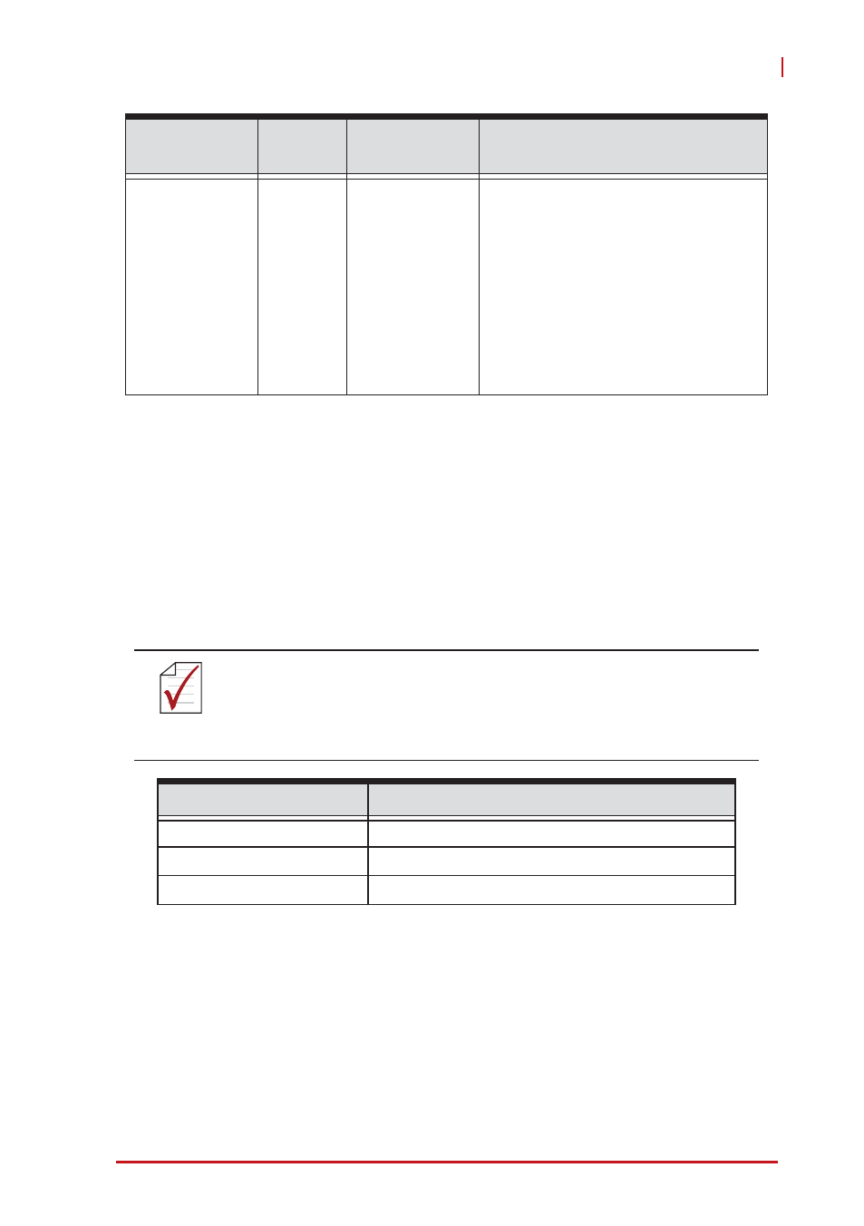
ReTrgCnt
31-bit
1-2147483647 Enables re-trigger to accept
multiple triggers.
X
1 - 2147483647 for
normal operation
X
1 - 65535 for Data
Average mode
See Acquisition with Re-
Triggering
NOTE:
NOTE:
Different signals cannot be routed onto the same trigger bus
line.
SSI Timing Signal
Function
SSI Clock (10MHz)
Input/output timebase signal through SSI
SSI Trig
Input/output trigger signal through SSI
SSI_pre_data_rdy
Input/output trigger signal through SSI
Counter
Name
Length
Valid Value
Description