2 unpacking, 3 pcb layout – ADLINK PCI-7432 User Manual
Page 17

Getting Started
•
9
2.2 Unpacking
The PCI-7432/33/34 card contains electro-static sensitive components that
can be easily be damaged by static electricity.
Therefore, the card should be handled on a grounded anti -static mat. The
operator should be wearing an anti -static wristband, grounded at the same
point as the anti-static mat.
Inspect the card module carton for obvious damages. Shipping and handling
may cause damage to your module. Be sure there are no shipping and
handling damages on the modules carton before continuing.
After opening the card module carton, extract the system module and place
it only on a grounded anti -static surface with component side up.
Again, inspect the module for damages. Press down on all the socketed IC's
to make sure that they are properly seated. Do this only with the module
place on a firm flat surface
Note: DO NOT ATTEMPT TO INSTALL A DAMAGED BOARD IN THE
COMPUTER.
You are now ready to install your card.
2.3 PCB Layout
2.3.1
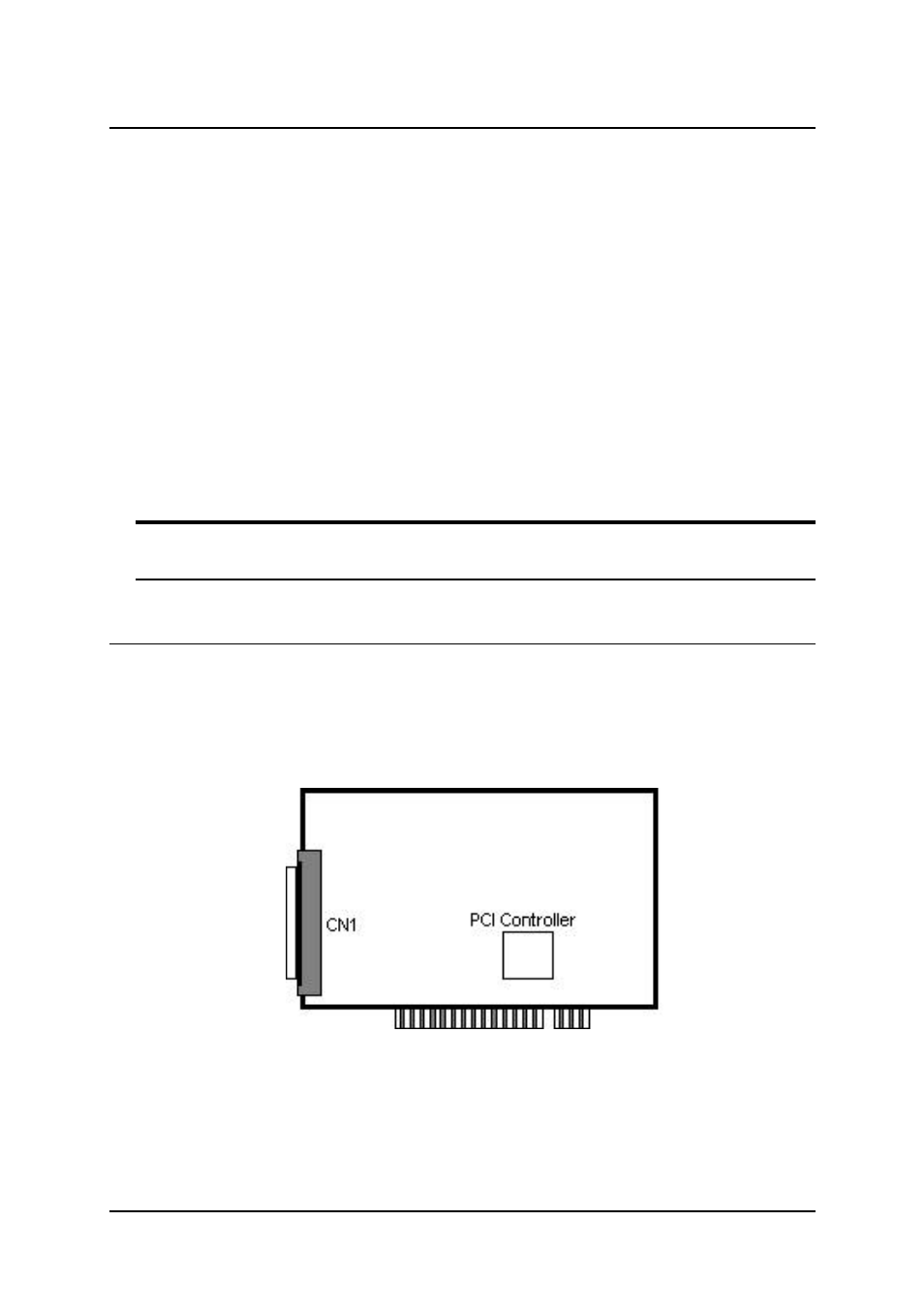
PCI-743X PCB Layout
CN1 is the I/O interface and is a 100-pin SCSI-type connector.
Figure 1: PCI-743X PCB Layout
