6 connector pin assignment – ADLINK PCM-6308V+ User Manual
Page 4
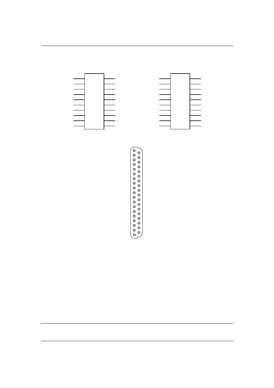
2.6 Connector Pin Assignment
The pin assignments of PCM-6308V+ are shown below:
DO3
DO2
DO1
DO0
GND
-15V
A.GND
N.C.
V7
A.GND
CN1
DI3
DI2
DI1
DI0
GND
ExtVref
+15V
A.GND
N.C.
V6
1
3
5
7
9
11
13
15
17
19
2
4
6
8
10
12
14
16
18
20
N.C.
V5
A.GND
N.C.
V3
A.GND
N.C.
V1
A.GND
A.GND
CN2
A.GND
N.C.
V4
A.GND
N.C.
V2
A.GND
N.C.
V0
A.GND
1
3
5
7
9
11
13
15
17
19
2
4
6
8
10
12
14
16
18
20
Pin Assignment of CN1 & CN2
DI3
DI2
DI1
DI0
GND
ExtVref
+15V
A.GND
(A6)
V6
A.GND
(A4)
V4
A.GND
(A2)
V2
A.GND
(A0)
V0
(1)
(2)
(3)
(4)
(5)
(6)
(7)
(8)
(9)
(10)
(11)
(12)
(13)
(14)
(15)
(16)
(17)
(18)
(19)
DO3
DO2
DO1
DO0
GND
-15V
A.GND
(A7)
V7
A.GND
(A5)
V5
A.GND
(A3)
V3
A.GND
(A1)
V1
(20)
(21)
(22)
(23)
(24)
(25)
(26)
(27)
(28)
(29)
(30)
(31)
(32)
(33)
(34)
(35)
(36)
(37)
Pin Assignment of 37-pin connector when using ACL-10337 Cable
Legend:
Vn
: the voltage output of channel n
for
PCM-6308V+,
n=0~7
ExtVref
: external reference voltage for voltage output
AGND
: Ground of analog output channels and +/-15V
-15V
: -15V voltage output
+15V
: +15V voltage output
DIx
: Digital input channel x
DOx
: Digital Output channel x
GND
: Isolated ground of digital input and output
N.C.
: No Connection
Note: Register format, operation theorem and C/C++ Libraries of PCM-6308V+ are the same as those
of the PCI-6308V, please refer to chapter 3~5 of the PCI-6308V manual for detailed information.