2 a/d data registers, 3 a/d channel multiplexer register – ADLINK ACL-8112 Series User Manual
Page 41
Registers
• 33
4.2 A/D Data Registers
The ACL-8112 series has a 12-bit resolution for each analog input channel,
the digital data is store in the A/D data registers after an A/D conversion.
The A/D data is put into two 8 bits registers. The lowest byte data (8 LSBs)
are placed in address BASE+4 and the highest byte data (4 MSBs) are
placed in address BASE+5. A DRDY bit is used to indicate the status of
the A/D conversion. When the DRDY goes low, it means an A/D
conversion is complete.
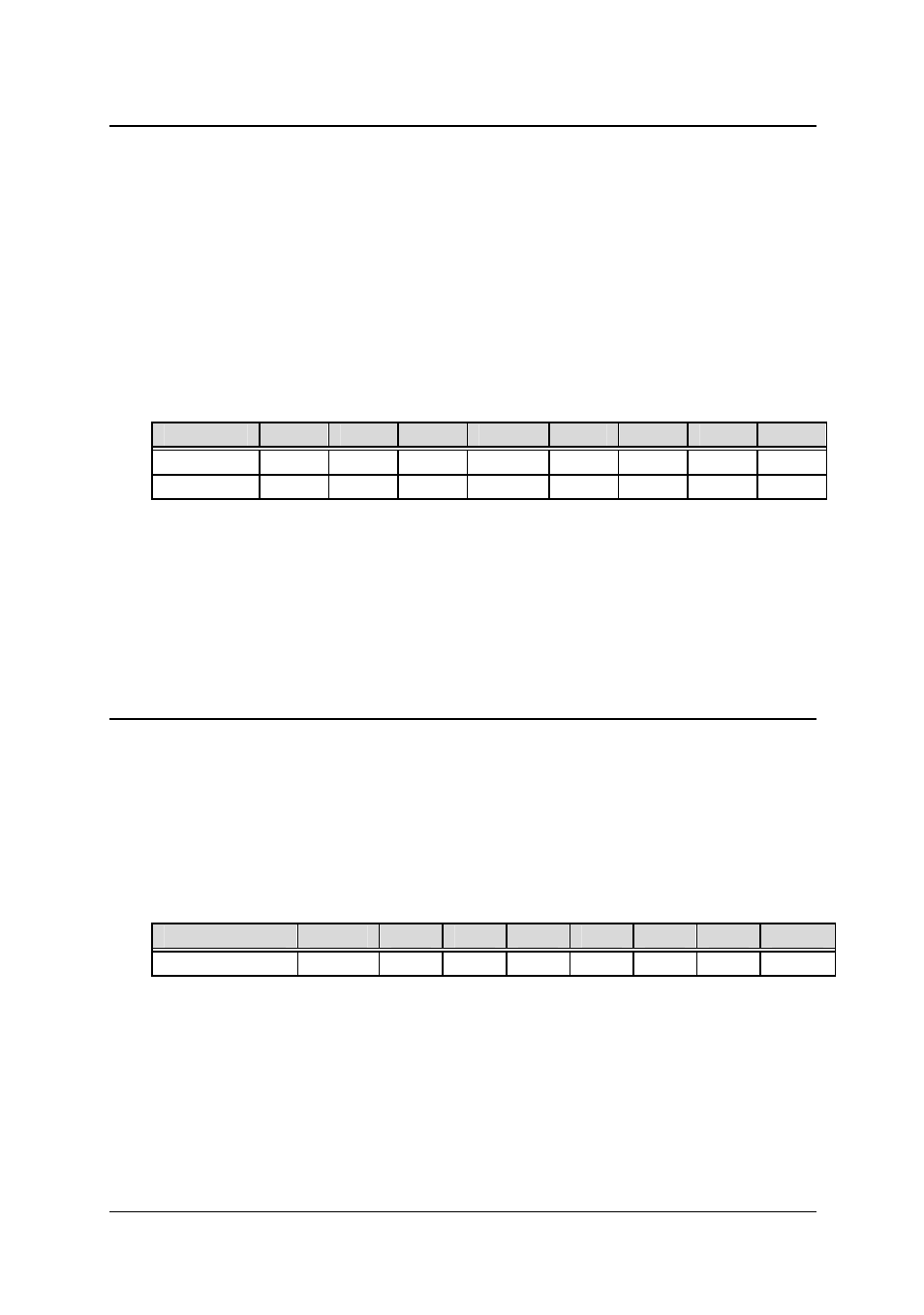
Address : BASE + 4 and BASE + 5
Attribute: read only
Data Format:
Bit
7
6
5
4
3
2
1
0
BASE+4 AD7 AD6 AD5 AD4 AD3 AD2 AD1 AD0
BASE+5 0
0 0 DRDY
AD11
AD10
AD9 AD8
AD11 …. AD0: Analog to digital data. AD11 is the Most Significant
Bit(MSB). AD0 is the Least Significant Bit(LSB).
DRDY: Data Ready Signal.
1: A/D data is not ready
0: A/D conversion is completed.
It will be set to 1, when reading the low byte.
4.3 A/D Channel Multiplexer Register
This register is used to control the A/D channels. It's a write only register.
When a channel number is written to the register, the multiplexer switches
to another channel and waits until there’s a conversion and switches again.
Address : BASE + 10
Attribute: write only
Data Format:
Bit
7
6
5
4
3
2
1
0
BASE+10
X
X CS1 CS0 CL3 CL2 CL1 CL0
CLn: multiplexer channel number (n=0~3).
CL3 is MSB, and CL0 is LSB.
CS0, CS1: Single-ended and Differential Selection (ACL-8112DG/HG only)