3 adc sampling rate and timebase control, 1 internal oscillator, 2 external clock through front panel – ADLINK PXI-2022 User Manual
Page 36: Adc sampling rate and timebase control, 28 function block and operation theory
28
Function Block and Operation Theory
4.3
ADC Sampling Rate and TIMEBASE Control
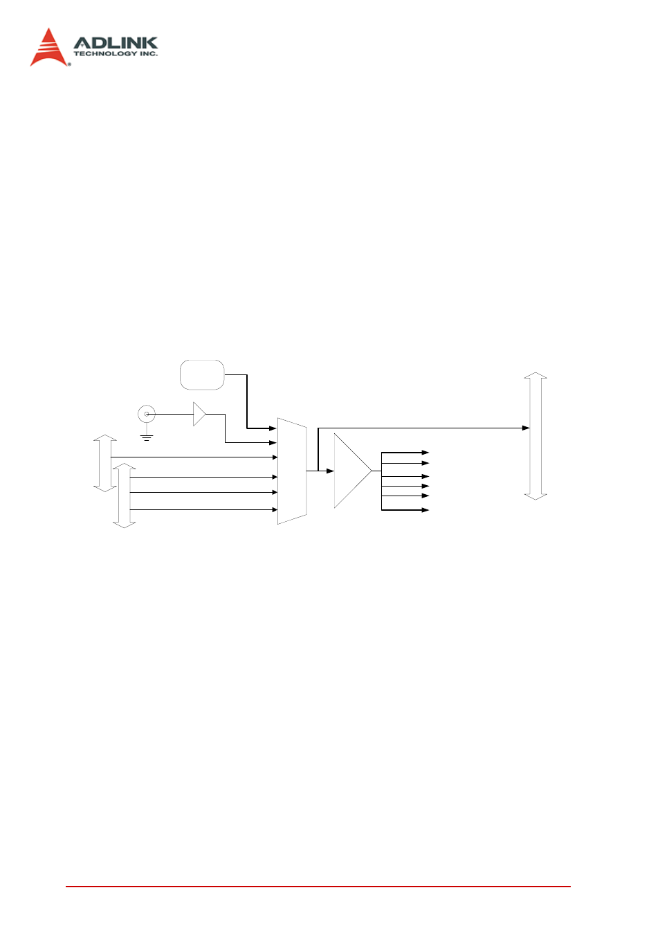
The PXI-2022 supports six timebase sources for analog input con-
version:
1. On board Internal oscillator
2. External clock through front panel (AFI[0..7])
3. External clock through front panel SMB CLK IN
4. PXI Star Trigger
5. PXI Trigger Bus Line 0
6. PXI 10M
The following diagram shows the timebase architecture of the PXI-
2022.
Figure 4-4: PXI-2022 Timebase Source and Architecture.
4.3.1
Internal Oscillator
The PXI-2020/2022 equips a high stability, low jitter oscillator for
the ADCs. The oscillators are 80 MHz for the PXI-2020/2022.
4.3.2
External Clock through Front Panel
When you need a specific timebase in some applications that the
onboard oscillator is not achievable, a clock from an external
device can replace onboard oscillator. In addition, external time-
base also provides a method to synchronize the DAQ module to
other measurement modules by distribut-ing/receiving a common
clock to/from multiple modules. The PXI-2020/2022 can receive
T
im
eb
ase
C
lo
ck
M
ux
P
X
I Inter
face
PXI Trigger Bus Line 0
PXI_STAR
Ext. CLK IN
SMB
Connector
ADC15
P
X
I Inter
face
PXI Trigger Bus Line 0
PXI_10M
Onboard
Oscillator
ADC0
ADC1
:
:
1-to
-1
6 Cloc
k
Bu
ffer
CLK Buffer
SC
SI
AFI[0..7]