2 a/d conversion, A/d conversion, Figure 3-2 – ADLINK USB-1210 User Manual
Page 32: Daughter board functional block diagram, Io connector, 40 pin board to board conn x2
22
Operation & Calibration
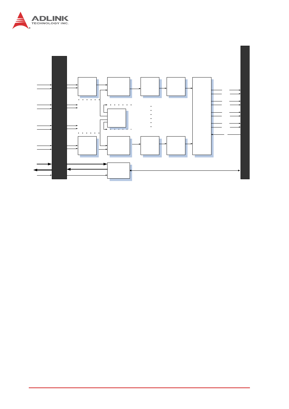
Figure 3-2: Daughter Board Functional Block Diagram
3.1.2
A/D Conversion
When using an A/D converter, the properties of the signal to be
measured must be considered and a channel and connection of
signals to the module selected. Please see Section 1.7: Analog
Input Signal Connection. As well, A/D signal configuration,
including channel, gain, and signal type must be defined and set.
A/D acquisition is initiated by a predefined trigger source. Data
acquisition will commence once a trigger condition is matched.
After A/D conversion, A/D data is buffered in a data FIFO for
transfer into system memory for further processing.
DC path/
Calibration Source
SW
PGA
Signal
Protection
2nd-order
LPF
1st CH
Four channels
ADC
4th CH
Calibration
Mux and
Reference Src
BUSY_CH0
2nd-order
LPF
PGA
IO Connector
AI CH0+
DC path/
Calibration Source
SW
Signal
Protection
AI CH0-
AI CH1+
AI CH1-
AI CH2+
AI CH2-
AI CH3+
AI CH3-
SCK
SDO_CH0
BUSY_CH1
SDO_CH1
BUSY_CH2
SDO_CH2
BUSY_CH3
SDO_CH3
40 Pin Board to Board Conn x2
DI
DO
Trigger
DIO
And
Trigger
DI CH[7..0]
DO CH[3..0]
AI TRIGGER