3 operation & calibration, 1 operation, 1 signal function – ADLINK USB-1210 User Manual
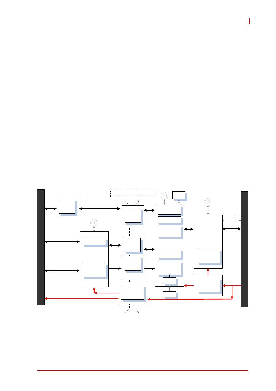
Page 31: Operation, Signal function, Figure 3-1, Carrier board functional block diagram, 3operation & calibration, Figure 3-1: carrier board functional block diagram, Usb interface

Operation & Calibration
21
USB-1210
3
Operation & Calibration
Operation of the USB-1210 is described here to assist in
configuration and programming of the module. Functions
described include A/D conversion, programmable function I/O,
and others
3.1 Operation
3.1.1
Signal Function
The USB-1210 provides 4 truly differential and
simultaneous-sampling analog input channels of 16-bit A/D input.
Each A/D input channel is connected to one ADC (LT LTC2380 or
equivalent). The ADC controller and all timing control logics are
implemented by the FPGA. The USB-1210 utilizes calibration
circuits to provide high performance and low-temperature drift
signal acquisition. Calibration data is saved in the EEPROM.
Figure 3-1: Carrier Board Functional Block Diagram
FPGA
ADC Control
Trigger Control
Data Processing
8051 Core
Function
PCIe Gen1
x4
FIFO
USB Interface
ADC BUS
PXIe_DSTARCp/n
USB Bus
USB BUS
+5V Supply
Cypress
CY7C68013A
8051 Core
12/24/48MHz
ADD/
DATA
24 MHz
XTAL
Power
Circuit
EEPROM
AI Calibration CTRL
CPLD SPI
BUS
Configuration
3.3V Supply
3.3V, 1.2V
Supply
40
Pin
Bo
ard to
Bo
ard
Conn
x2
Isolation
Power
Circuit
Isolation Moat
Isolator
Circuit
Isolator
Circuit
CPLD
ADC SPI BUS
AI Configuration
66 MHz
OSC
Isolated
CPLD SPI
BUS
Isolated
ADC BUS
ADC SPI
DIO
And
Trigger
AI Configuration
Isolated 3.3V
Supply
Isolated +13V, -13V
Supply
DIO
DI
DO
Trigger
GPTC
Configuration
Isolator
Circuit
Isolated
DIO and Trigger
80 MHz
OSC
DDR3
