Figure 8. pulse width register – CH Tech Pulse Generator User Manual
Page 18
12
Delay Register (0A) This read/write register controls delay of the primary pulse from the trigger
out or the delay of the second pulse of a double pulse from the trigger out. See Figure 7 for
details.
0A
Delay Register
Bit
15
14
13
12
11
10
9
8
7
6
5
4
3
2
1
0
Write
Not Used
Delay Multiplier
Read
Not Used
Delay Multiplier
Delay Multiplier
Delay Multiplier (period = Delay Multiplier
PRI Range)
NOTES:
1) The Range field is programmable in the PRI register.
2) The minimum delay multiplier is 1; therefore, the minimum programmable delay is 25
ns.
3) The maximum delay multiplier is 1023, however do not set the Delay
Pulse Width
greater than the PRI Period
75 nsec.
4) For highest accuracy use the smallest PRI range with a larger multiplier.
Figure 7. Delay Register
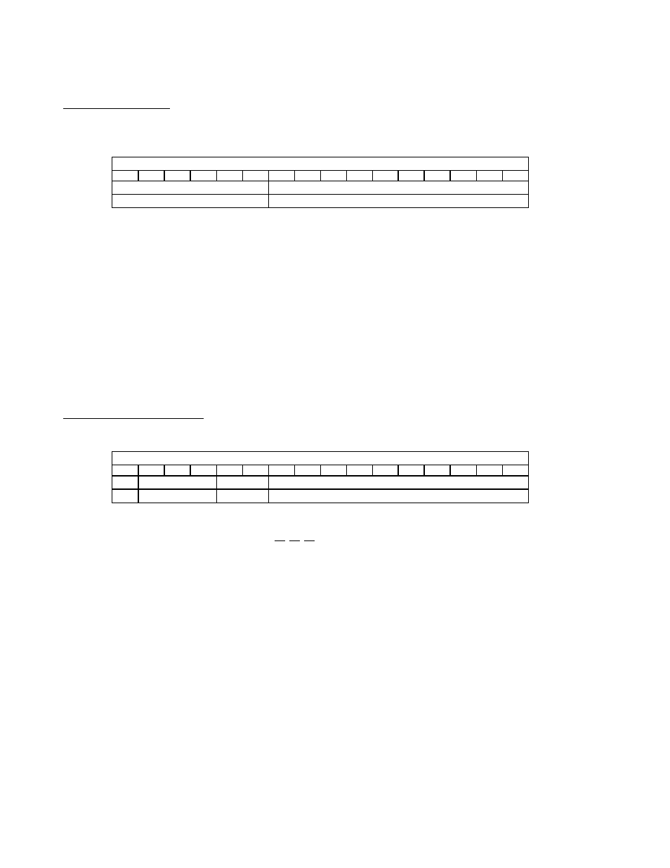
Pulse Width Register (0C) This read/write register controls the pulse width of the output pulse.
See Figure 8 for details.
0C
Pulse Width Register
Bit
15
14
13
12
11
10
9
8
7
6
5
4
3
2
1
0
Write
N/U
Range
Not Used
PW Multiplier
Read
N/U
Range
Not Used
PW Multiplier
N/U
Not Used
Range
PW Range
bit
14 13 12
0 0 0 25 ns
0 0 1 100 ns
0 1 0 1
s
0 1 1 10
s
1 0 0 100
s
1 0 1 1 ms
1 1 X invalid
PW Multiplier
PW Multiplier (width = PW Multiplier
Range)
NOTES:
1) The minimum programmable pulse width period is 25 nsec.
2) The pulse typically requires 75 nsec to start after trigger out or the delay time-out.
3) The maximum pulse width multiplier is 1023, however do not program the Delay +
Pulse Width greater than the PRI period
75 nsec.
4) For highest accuracy use the smallest range with a larger multiplier.
Figure 8. Pulse Width Register