Figure 3. hardware configurable controls – CH Tech Pulse Generator User Manual
Page 13
7
3.0
FUNCTIONAL DESCRIPTION
3.1
GENERAL
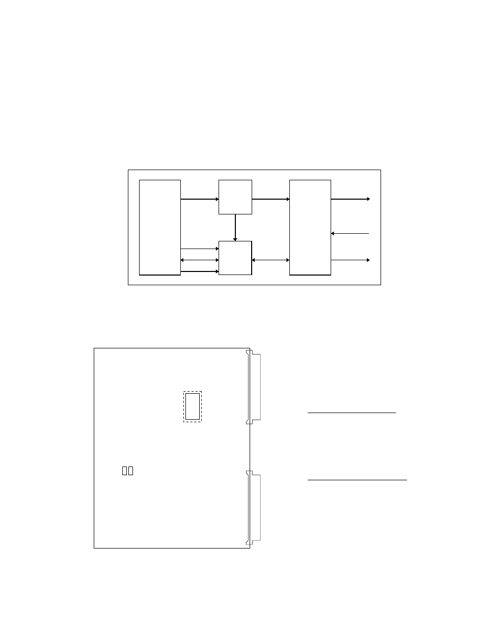
The VX462B is configured, controlled, and statused through on-board registers accessible
through the VXI backplane. These registers control the mode of operation, pulse repetition
interval, pulse width, delay time, output amplitude and an output relay. A simplified block
diagram of the module is shown in Figure 2.
CONTROL
DATA BUS
ADDR BUS
ADDR BUS
CONTROL
DATA BUS
TRIG OUT
TRIG IN/GATE
PULSE OUT
LOGIC
CONTROL
ADDRESS
DECODE
VXI &
USER
REGISTERS
PULSE
GENERATOR
LOGIC
VXI
INTERFACE
Figure 2. Simplified Block Diagram
3.2
SWITCHES AND JUMPERS
The following switches are used to
configure the VX462B. Refer to
Figure 3 for the switch and jumper
locations.
LOGICAL ADDRESS An 8-bit
logical address switch is provided
to uniquely identify the module in
the system. Refer to Section 4 for
switch definition.
OUTPUT IMPEDANCE The
VX462B can be configured with a
50 Ohm or a 2 Ohm output
impedance. Install a jumper in J5
only for 2 Ohms, and J6 only for
50 Ohm series output impedance.
Logical Address
Selection
128
1
0
1
P1
P2
J6
J5
50 Ohm
2 Ohm
Output Impedance
Selection
Figure 3. Hardware Configurable Controls