CH Tech Pulse Generator User Manual
Page 15
9
3.5
CONFIGURATION REGISTERS
There are several types of registers used to configure and control the VX462B. The VXI
configuration registers provide for control and status as required by the VXIbus specification.
The other register provides board-level control and status of the pulse repetition interval, pulse
width, trigger modes and delay times, and output amplitude. An address map of the registers is
shown in Table I.
3.5.1 VXI Configuration Registers
The VXI configuration registers contain basic information needed to configure a VXIbus system.
The configuration information includes: manufacturer identification, product model code, device
type, memory requirements, device status, and device control. The registers are briefly described
below and are detailed in Figure 5.
VXI Identification (ID) Register (Base + 00h) - A read of this register provides
manufacturer identification, device classification (i.e., register based), and the addressing
mode (A16). A write to this register has no effect.
VXI Device Type Register (Base + 02h) - A read of this register provides the model code
identifier. A write to this register has no effect.
VXI Status/Control Register (Base + 04h) - A read of this register provides the state of
P2 MODID* line, and the Ready and self-test Passed status. A write to bit 0 of this
register provides a reset of the module. SYSFAIL* is not implemented on this module.
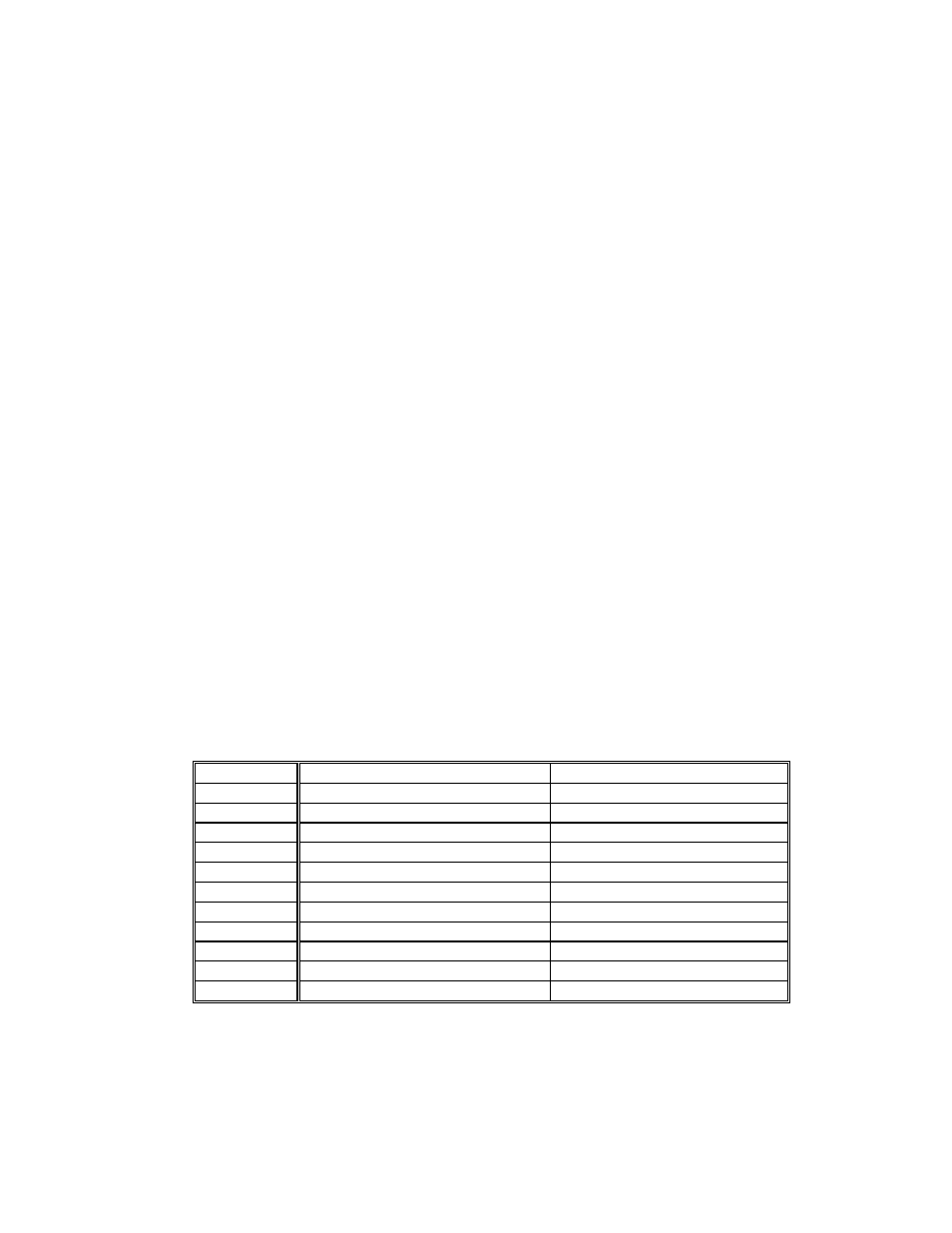
Table I. VXI Register Address Map
A16 Address
Write Register Description
Read Register Description
Base + 12
High Reference Register
High Reference Register
Base + 10
Low Reference Register
Low Reference Register
Base + 0E
Pulse Control Register
Pulse Control Register
Base + 0C
Pulse Width Register
Pulse Width Register
Base + 0A
Delay Register
Delay Register
Base + 08
PRI Register
PRI Register
Base + 06
VXI Unused Register
VXI Unused Register
Base + 04
VXI Control Register
VXI Status Register
Base + 02
VXI Read Only Register
VXI Device Type Register
Base + 00
VXI Read Only Register
VXI ID Register
Bit
D15 . . . . . D00
D15 . . . . . D00