Ad620, Warning – Analog Devices AD620 User Manual
Page 4
AD620
REV. E
–4–
NOTES
1
Stresses above those listed under Absolute Maximum Ratings may cause perma-
nent damage to the device. This is a stress rating only; functional operation of the
device at these or any other conditions above those indicated in the operational
section of this specification is not implied. Exposure to absolute maximum rating
conditions for extended periods may affect device reliability.
2
Specification is for device in free air:
8-Lead Plastic Package:
θ
JA
= 95
°
C/W
8-Lead Cerdip Package:
θ
JA
= 110
°
C/W
8-Lead SOIC Package:
θ
JA
= 155
°
C/W
ABSOLUTE MAXIMUM RATINGS
1
Supply Voltage . . . . . . . . . . . . . . . . . . . . . . . . . . . . . . . . .
±
18 V
Internal Power Dissipation
2
. . . . . . . . . . . . . . . . . . . . . 650 mW
Input Voltage (Common Mode) . . . . . . . . . . . . . . . . . . . .
±
V
S
Differential Input Voltage . . . . . . . . . . . . . . . . . . . . . . . .
±
25 V
Output Short Circuit Duration . . . . . . . . . . . . . . . . . Indefinite
Storage Temperature Range (Q) . . . . . . . . . . –65
°
C to +150
°
C
Storage Temperature Range (N, R) . . . . . . . . –65
°
C to +125
°
C
Operating Temperature Range
AD620 (A, B) . . . . . . . . . . . . . . . . . . . . . . – 40
°
C to +85
°
C
AD620 (S) . . . . . . . . . . . . . . . . . . . . . . . . – 55
°
C to +125
°
C
Lead Temperature Range
(Soldering 10 seconds) . . . . . . . . . . . . . . . . . . . . . . . +300
°
C
ORDERING GUIDE
Model
Temperature Ranges Package Options*
AD620AN
– 40
°
C to +85
°
C
N-8
AD620BN
– 40
°
C to +85
°
C
N-8
AD620AR
– 40
°
C to +85
°
C
SO-8
AD620AR-REEL
– 40
°
C to +85
°
C
13" REEL
AD620AR-REEL7 – 40
°
C to +85
°
C
7" REEL
AD620BR
– 40
°
C to +85
°
C
SO-8
AD620BR-REEL
– 40
°
C to +85
°
C
13" REEL
AD620BR-REEL7 – 40
°
C to +85
°
C
7" REEL
AD620ACHIPS
– 40
°
C to +85
°
C
Die Form
AD620SQ/883B
–55
°
C to +125
°
C
Q-8
*N = Plastic DIP; Q = Cerdip; SO = Small Outline.
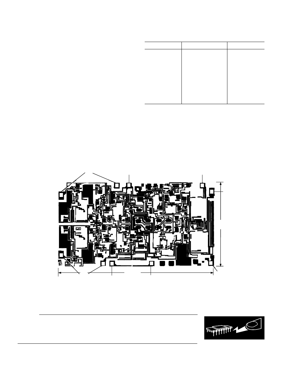
METALIZATION PHOTOGRAPH
Dimensions shown in inches and (mm).
Contact factory for latest dimensions.
+V
S
OUTPUT
REFERENCE
+IN
–V
S
–IN
*FOR CHIP APPLICATIONS: THE PADS 1R
G
AND 8R
G
MUST BE CONNECTED IN PARALLEL
TO THE EXTERNAL GAIN REGISTER R
G
. DO NOT CONNECT THEM IN SERIES TO R
G
. FOR
UNITY GAIN APPLICATIONS WHERE R
G
IS NOT REQUIRED, THE PADS 1R
G
MAY SIMPLY
BE BONDED TOGETHER, AS WELL AS THE PADS 8R
G
.
4
5
6
7
8
8
R
G
*
1
1
2
3
R
G
*
0.125
(3.180)
0.0708
(1.799)
CAUTION
ESD (electrostatic discharge) sensitive device. Electrostatic charges as high as 4000 V readily
accumulate on the human body and test equipment and can discharge without detection.
Although the AD620 features proprietary ESD protection circuitry, permanent damage may
occur on devices subjected to high energy electrostatic discharges. Therefore, proper ESD
precautions are recommended to avoid performance degradation or loss of functionality.
WARNING!
ESD SENSITIVE DEVICE