An352, Gate drive external components, Pcb layout – Cirrus Logic AN352 User Manual
Page 2: Summary, Gd c, Gd b

AN352
2
AN352REV1
3. Gate Drive External Components
High voltage MOSFETs generally have low gate-charge capacitance. As a result, they can be driven directly from the IC. The
CS1501 & CS1601 are designed to function as power factor corrected SMPS working in discontinuous mode (DCM). They are
best suited for supplies less than150 W. With relatively low switching frequencies (<70kHz) and low switching current, the ben-
efits of having very fast rise & fall times is reduced.
-
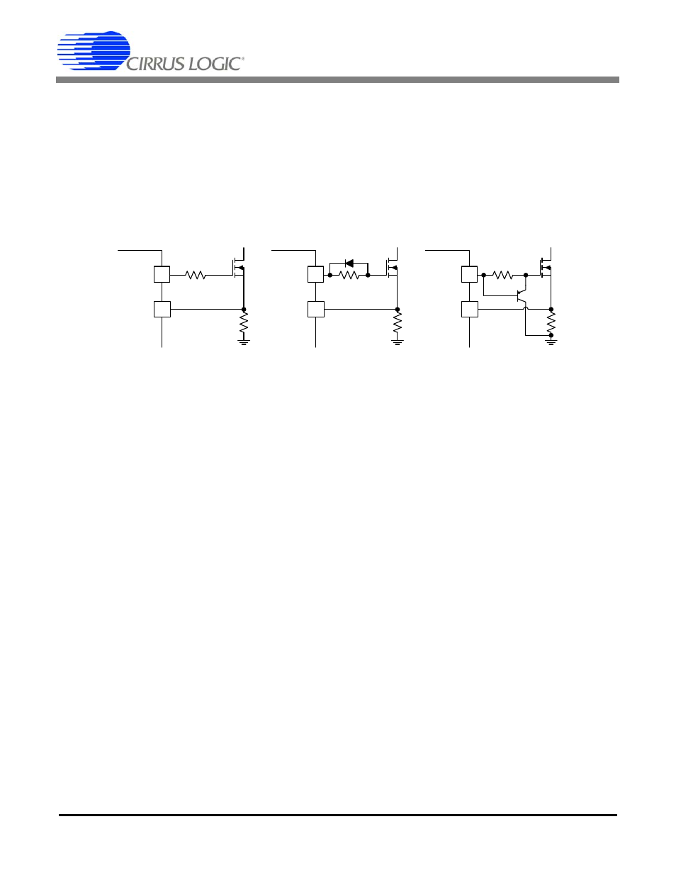
The simplest implementation is a low-value resistor (~10
Ω) in series with the driver & MOSFET gate. (Option A.)
-
Efficiency can be improved by adding a diode in parallel with the resistor. (Option B.) This turns the MOSFET off quickly,
and reduces the I – V losses as the voltage rises while current is still flowing.
-
Adding a small-signal PNP transistor further reduces turn off time. (Option C.)
4. PCB Layout
The IC should be placed as close as possible to the MOSFET, with a short, direct connection from the driver to the gate. The
return path from the FET source to the IC should also be minimal. This reduces issues with PCB trace impedance interfering with
the drive — both resistive and inductive. For further details, please refer to Cirrus Logic application note AN350, CS1601 Layout
Guidelines.
5. Summary
Simple gate drive structures are sufficient for most PFC applications. A choice from one of the schemes listed above will work,
with focus on following basic layout rules.
A
7
R
g
7
GD
C
7
R
g
7
GD
B
7
R
g
7
GD
7
4
CS
7
4
CS
7
4
CS
R
cs
R
cs
R
cs
Q
off
D
off
